SLVS529D April 2004 – January 2015 TL1431-EP
PRODUCTION DATA.
- 1 Features
- 2 Applications
- 3 Description
- 4 Simplified Schematic
- 5 Revision History
- 6 Pin Configuration and Functions
- 7 Specifications
- 8 Parameter Measurement Information
- 9 Detailed Description
- 10Application and Implementation
- 11Power Supply Recommendations
- 12Layout
- 13Device and Documentation Support
- 14Mechanical, Packaging, and Orderable Information
Package Options
Mechanical Data (Package|Pins)
- D|8
Thermal pad, mechanical data (Package|Pins)
Orderable Information
7 Specifications
7.1 Absolute Maximum Ratings(1)
over operating free-air temperature range (unless otherwise noted)| MIN | MAX | UNIT | ||
|---|---|---|---|---|
| Cathode voltage(2), VKA | 37 | V | ||
| Continuous cathode current, IKA | –100 | 150 | mA | |
| Reference input current, II(ref) | –0.00005 | 10 | mA | |
| Operating virtual junction temperature(3), TJ | 150 | °C | ||
| Lead temperature 1.6 mm (1/16 inch) from case for 10 s | 260 | °C | ||
| Storage temperature, Tstg | –65 | 150 | °C | |
(1) Stresses beyond those listed under Absolute Maximum Ratings may cause permanent damage to the device. These are stress ratings only, and functional operation of the device at these or any other conditions beyond those indicated under Recommended Operating Conditions is not implied. Exposure to absolute-maximum-rated conditions for extended periods may affect device reliability.
(2) All voltage values are with respect to ANODE, unless otherwise noted.
(3) Long-term high-temperature storage and/or use at the absolute maximum ratings may result in a reduction of overall device life. See www.ti.com/ep_quality for additional information on enhanced plastic packaging.
7.2 ESD Ratings
| VALUE | UNIT | |||
|---|---|---|---|---|
| V(ESD) | Electrostatic discharge | Human body model (HBM), per ANSI/ESDA/JEDEC JS-001, all pins(1) | ±4000 | V |
| Charged device model (CDM), per JEDEC specification JESD22-C101, all pins(2) | ±2000 | |||
(1) JEDEC document JEP155 states that 500-V HBM allows safe manufacturing with a standard ESD control process.
(2) JEDEC document JEP157 states that 250-V CDM allows safe manufacturing with a standard ESD control process.
7.3 Recommended Operating Conditions
| MIN | MAX | UNIT | ||
|---|---|---|---|---|
| VKA | Cathode voltage | VI(ref) | 36 | V |
| IKA | Cathode current | 1 | 100 | mA |
| TA | Operating free-air temperature | –55 | 125 | °C |
7.4 Thermal Information
| THERMAL METRIC(1) | TL1431-EP | UNIT | |
|---|---|---|---|
| D | |||
| 8 PINS | |||
| RθJA(high) | Junction-to-ambient thermal resistance (high K board) | 97 | °C/W |
| RθJA(low) | Junction-to-ambient thermal resistance (low K board) | 165 | |
(1) For more information about traditional and new thermal metrics, see the IC Package Thermal Metrics application report, SPRA953.
7.5 Dissipation Rating Table
| PACKAGE | TA ≤ 25°C POWER RATING |
PACKAGE THERMAL IMPEDANCE | DERATING FACTOR ABOVE TA = 25°C |
TA = 70°C ABSOLUTE MAXIMUM POWER RATING |
TA = 85°C ABSOLUTE MAXIMUM POWER RATING |
TA = 125°C ABSOLUTE MAXIMUM POWER RATING |
|---|---|---|---|---|---|---|
| D | 1102 mW | 97°C/W (High K board) | 10 mW/°C | 824 mW | 670 mW | 257 mW |
| 165°C/W (Low K board) | 6 mW/°C | 484 mW | 393 mW | 151 mW |
7.6 Electrical Characteristics
at specified free-air temperature, IKA = 10 mA (unless otherwise noted)| PARAMETER | TEST CONDITIONS | TA(1) | TEST CIRCUIT | MIN | TYP | MAX | UNIT | ||
|---|---|---|---|---|---|---|---|---|---|
| VI(ref) | Reference input voltage | VKA = VI(ref) | 25°C | Figure 8 | 2490 | 2500 | 2510 | mV | |
| Full range | 2470 | 2530 | |||||||
| VI(dev) | Deviation of reference input voltage over full temperature range(2) | VKA = VI(ref) | Full range | Figure 8 | 17 | mV | |||
 |
Ratio of change in reference input voltage to the change in cathode voltage | ΔVKA = 3 to 36 V | Full range | Figure 9 | –1.1 | –2 | mV/V | ||
| II(ref) | Reference input current | R1 = 10 kΩ, | R2 = ∞ | 25°C | Figure 9 | 1.5 | 2.5 | μA | |
| Full range | 4 | ||||||||
| II(dev) | Deviation of reference input current over full temperature range(2) | R1 = 10 kΩ, | R2 = ∞ | Full range | Figure 9 | 0.5 | μA | ||
| Imin | Minimum cathode current for regulation | VKA = VI(ref) | 25°C | Figure 8 | 0.45 | 1 | mA | ||
| Ioff | Off-state cathode current | VKA = 36 V, | VI(ref) = 0 | 25°C | Figure 10 | 0.18 | 0.5 | μA | |
| Full range | 2 | ||||||||
| |zKA| | Output impedance(3) | VKA = VI(ref), ƒ ≤ 1 kHz, IKA = 1 to 100 mA |
25°C | Figure 8 | 0.2 | 0.4 | Ω | ||
(1) Full range is –40°C to 125°C for Q-suffix devices; –55°C to 125°C for M-suffix devices.
(2) The deviation parameters VI(dev) and II(dev) are defined as the differences between the maximum and minimum values obtained over the rated temperature range. The average full-range temperature coefficient of the reference input voltage  is defined as:
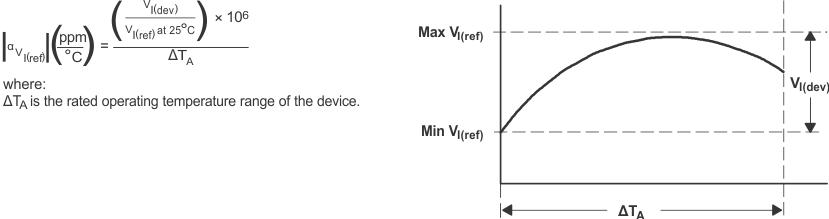
 is positive or negative, depending on whether minimum VI(ref) or maximum VI(ref), respectively, occurs at the lower temperature.
is defined as:
is positive or negative, depending on whether minimum VI(ref) or maximum VI(ref), respectively, occurs at the lower temperature.(3) The output impedance is defined as: 
When the device is operating with two external resistors (see Figure 9), the total dynamic impedance of the circuit is given by:
 , which is approximately equal to
 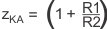 .
.
When the device is operating with two external resistors (see Figure 9), the total dynamic impedance of the circuit is given by:
, which is approximately equal to .7.7 Typical Characteristics
Data at high and low temperatures are applicable only within the recommended operating free-air temperature range.Table 1. Table of Graphs
| GRAPH TITLE | FIGURE |
|---|---|
| Reference voltage vs Free-Air Temperature | Figure 1 |
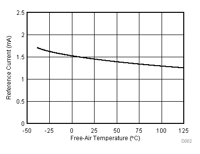
| Reference current vs Free-Air Temperature | Figure 2 |
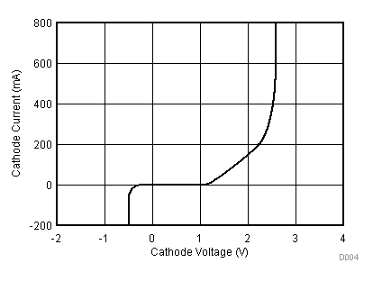
| Cathode Current vs Cathode Voltage | Figure 3, Figure 4 |
| Off-State Cathode Current vs Free-Air Temperature | Figure 5 |
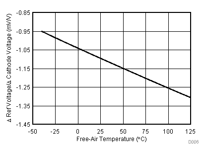
| Ratio of Delta Reference Voltage to Delta Cathode Voltage vs Free-Air Temperature | Figure 6 |
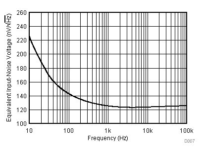
| Equivalent Input-Noise Voltage vs Frequency | Figure 7 |
| Equivalent Input-Noise Voltage Over a 10-s Period | Figure 11 |
| Small-Signal Voltage Amplification vs Frequency | Figure 13 |
| Reference Impedance vs Frequency | Figure 15 |
| Pulse Response | Figure 17 |
| Stability Boundary Conditions | Figure 19 |
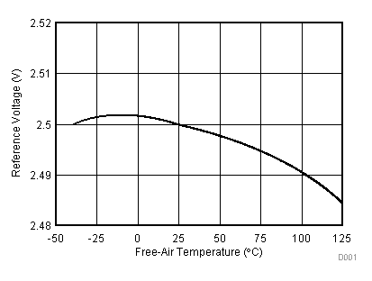
| VI(ref) = VKA | IKA = 10 mA | |
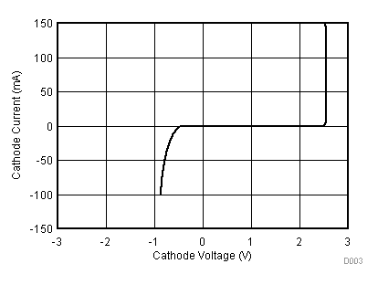
| VKA = VI(ref) | TA = 25°C | |
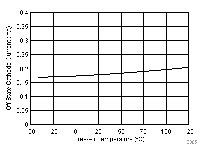
| VKA = 36 V | VI(ref) = 0 | |
| IO = 10 mA | TA = 25°C | |
| IKA = 10 mA | R1 = 10 kΩ | R2 = ∞ |
| VKA = VI(ref) | TA = 25°C | |
| VKA = 3 to 36 V | ||