SLVS038I January 1989 – July 2016 TL2842 , TL2843 , TL2844 , TL2845 , TL3842 , TL3843 , TL3844 , TL3845
PRODUCTION DATA.
- 1 Features
- 2 Applications
- 3 Description
- 4 Revision History
- 5 Pin Configuration and Functions
- 6 Specifications
- 7 Detailed Description
- 8 Application and Implementation
- 9 Power Supply Recommendations
- 10Layout
- 11Device and Documentation Support
- 12Mechanical, Packaging, and Orderable Information
Package Options
Refer to the PDF data sheet for device specific package drawings
Mechanical Data (Package|Pins)
- D|14
- D|8
- P|8
Thermal pad, mechanical data (Package|Pins)
Orderable Information
7 Detailed Description
7.1 Overview
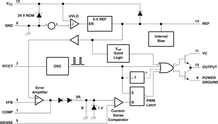
The TL284x and TL384x series of control integrated circuits provide the features that are necessary to implement off-line or DC-to-DC fixed-frequency current-mode control schemes, with a minimum number of external components. Some of the internally implemented circuits are an undervoltage lockout (UVLO), featuring a start-up current of less than 1 mA, and a precision reference trimmed for accuracy at the error amplifier input. Other internal circuits include logic to ensure latched operation, a pulse-width modulation (PWM) comparator (that also provides current-limit control), and a totem-pole output stage designed to source or sink high-peak current. The output stage, suitable for driving N-channel MOSFETs, is low when it is in the off state.
Major differences between members of these series are the UVLO thresholds and maximum duty-cycle ranges. Typical UVLO thresholds of 16 V (on) and 10 V (off) on the TLx842 and TLx844 devices make them ideally suited to off-line applications. The corresponding typical thresholds for the TLx843 and TLx845 devices are 8.4 V (on) and 7.6 V (off). The TLx842 and TLx843 devices can operate to duty cycles approaching 100%. A duty-cycle range of 0 to 50% is obtained by the TLx844 and TLx845 by the addition of an internal toggle flip-flop, which blanks the output off every other clock cycle.
The TL284x-series devices are characterized for operation from −40°C to +85°C. The TL384x devices are characterized for operation from 0°C to 70°C.
7.2 Functional Block Diagram

7.3 Feature Description
7.3.1 Pulse-by-Pulse Current Limiting
Pulse-by-pulse limiting is inherent in the control scheme. An upper limit on the peak current can be established by simply clamping the error voltage. Accurate current limiting allows optimization of magnetic and power semiconductor elements while ensuring reliable supply operation
7.3.2 Error Amplifier With Low Output Resistance
With a low output resistance, various impedance networks may be used on the compensation pin input for error amplifier feedback.
7.3.3 High-Current Totem-Pole Output
The output of the TLx84x devices can sink or source up to 1 A of current.
7.4 Device Functional Modes
7.4.1 Shutdown Technique
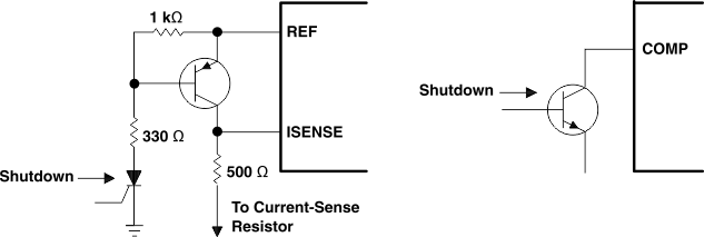
The PWM controller (see Figure 11) can be shut down by two methods: either raise the voltage at ISENSE above 1 V or pull the COMP terminal below a voltage two diode drops above ground. Either method causes the output of the PWM comparator to be high (see Functional Block Diagram). The PWM latch is reset dominant so that the output remains low until the next clock cycle after the shutdown condition at the COMP or ISENSE terminal is removed. In one example, an externally latched shutdown can be accomplished by adding an SCR that resets by cycling VCC below the lower UVLO threshold. At this point, the reference turns off, allowing the SCR to reset.
 Figure 11. Shutdown Techniques
7.4.2 Slope Compensation
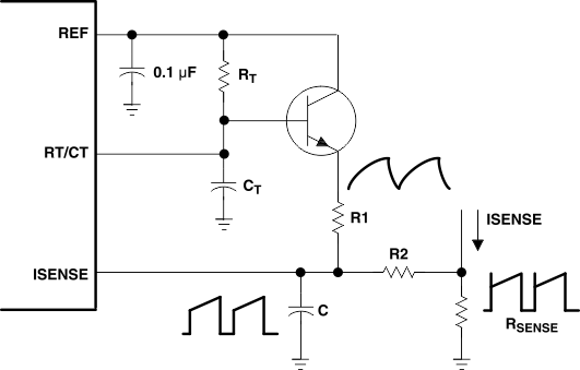
A fraction of the oscillator ramp can be summed resistively with the current-sense signal to provide slope compensation for converters requiring duty cycles over 50% (see Figure 12).
NOTE
Capacitor C forms a filter with R2 to suppress the leading-edge switch spikes.
 Figure 12. Slope Compensation