SLVS004I April 1979 – August 2016 TL317
PRODUCTION DATA.
- 1 Features
- 2 Applications
- 3 Description
- 4 Revision History
- 5 Pin Configuration and Functions
- 6 Specifications
- 7 Detailed Description
-
8 Application and Implementation
- 8.1 Application Information
- 8.2
Typical Applications
- 8.2.1 Adjustable Voltage Regulator
- 8.2.2 0-V to 30-V Regulator Circuit
- 8.2.3 Regulator Circuit With Improved Ripple Rejection
- 8.2.4 Precision Current-Limiter Circuit
- 8.2.5 Tracking Preregulator Circuit
- 8.2.6 Slow-Turnon 15-V Regulator Circuit
- 8.2.7 50-mA Constant-Current Battery-Charger Circuit
- 8.2.8 Current-Limited 6-V Charger
- 8.2.9 High-Current Adjustable Regulator
- 9 Power Supply Recommendations
- 10Layout
- 11Device and Documentation Support
- 12Mechanical, Packaging, and Orderable Information
Package Options
Mechanical Data (Package|Pins)
Thermal pad, mechanical data (Package|Pins)
- PS|8
Orderable Information
10 Layout
10.1 Layout Guidelines
- It is recommended that the input terminal be bypassed to ground with a bypass capacitor.
- The optimum placement for the bypass capacitor is closest to the input terminal of the device and the system GND. Take care to minimize the loop area formed by the bypass-capacitor connection, the input terminal, and the system GND.
- For operation at full rated load, it is recommended to use wide trace lengths to eliminate I × R drop and heat dissipation.
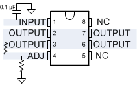
10.2 Layout Example
 Figure 14. TL317D Layout Example