SLVS765B October 2008 – September 2015 TLC5925
PRODUCTION DATA.
- 1 Features
- 2 Applications
- 3 Description
- 4 Revision History
- 5 Pin Configuration and Functions
-
6 Specifications
- 6.1 Absolute Maximum Ratings
- 6.2 ESD Ratings
- 6.3 Recommended Operating Conditions
- 6.4 Thermal Information
- 6.5 Electrical Characteristics: VDD = 3 V
- 6.6 Electrical Characteristics: VDD = 5.5 V
- 6.7 Power Dissipation and Thermal Impedance
- 6.8 Timing Requirements
- 6.9 Switching Characteristics: VDD = 3 V
- 6.10 Switching Characteristics: VDD = 5.5 V
- 6.11 Typical Characteristics
- 7 Parameter Measurement Information
- 8 Detailed Description
- 9 Application and Implementation
- 10Power Supply Recommendations
- 11Layout
- 12Device and Documentation Support
- 13Mechanical, Packaging, and Orderable Information
Package Options
Mechanical Data (Package|Pins)
Thermal pad, mechanical data (Package|Pins)
- DW|24
Orderable Information
9 Application and Implementation
NOTE
Information in the following applications sections is not part of the TI component specification, and TI does not warrant its accuracy or completeness. TI’s customers are responsible for determining suitability of components for their purposes. Customers should validate and test their design implementation to confirm system functionality.
9.1 Application Information
9.1.1 Turning on the LEDs
To turn on an LED connected to one of the outputs of the device, the output must be pulled low. To do this, the SDI signal must let the device know which outputs should be activated. Using the rising edge of CLK, the logic level of the SDI signal latches the desired state of each output into the shift register. Once this is complete, the LE signal must be toggled from low to high then back to low. Once /OE is pulled down, the corresponding outputs will be pulled low and the LEDs will be turned on. The below diagram shows outputs 0, 3, 4, 5, 10, 13, and 15 being activated.
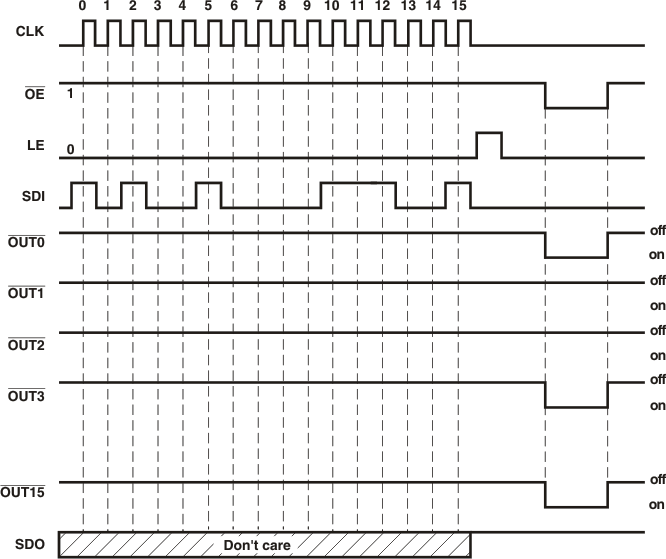 Figure 6. Timing Diagram
9.1.2 Propagation Delay Times
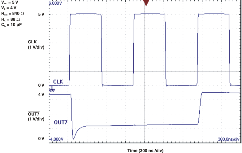 Figure 7. CLK to OUT7
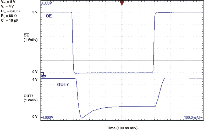 Figure 9. OE to OUT7
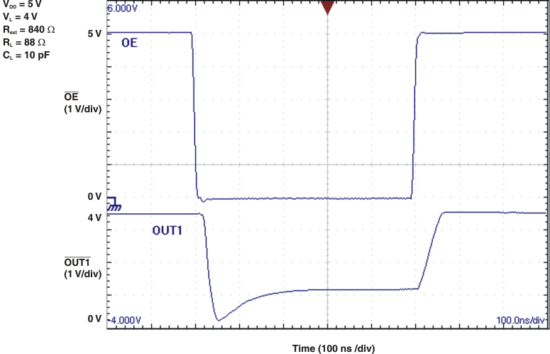 Figure 8. OE to OUT1
9.2 Typical Application
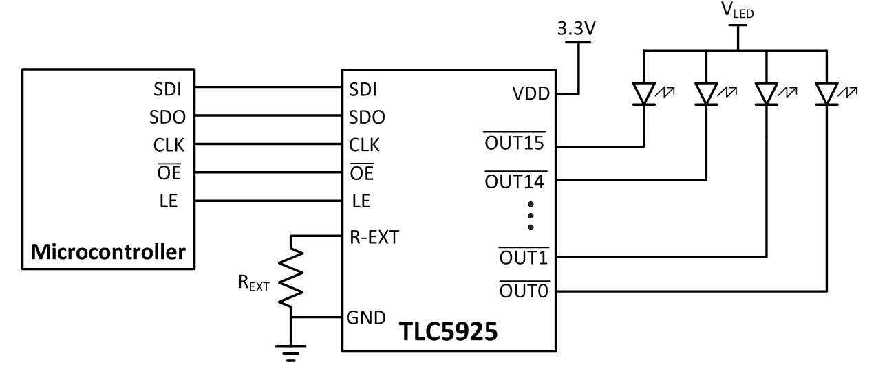
9.2.1 Design Requirements
For the following design procedure, the input voltage (VDD) is between 3 V and 5.5 V.
9.2.2 Detailed Design Procedure
9.2.2.1 Adjusting Output Current
TLC5925 sets IOUT based on the external resistor Rext. Users can follow the below formulas to calculate the target output current IOUT,target in the saturation region:
IOUT,target = (1.21 V / Rext) × 18, where Rext is the external resistance connected between R-EXT and GND.
Therefore, the default current is approximately 26 mA at 840 Ω and 13 mA at 1680 Ω.
9.2.3 Application Curve
The default relationship after power on between IOUT,target and Rext is shown in Figure 10.
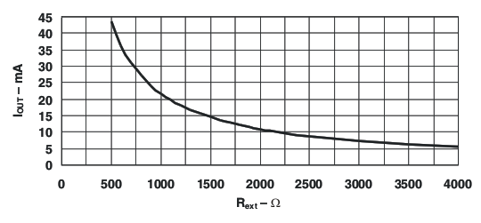 Figure 10. Default Relationship Curve Between IOUT,target and Rext After Power Up