SBVS222C February   2013  – October 2016 TLC59731

PRODUCTION DATA.  

  1. Features
  2. Applications
  3. Description
  4. Revision History
  5. Pin Configuration and Functions
  6. Specifications
    1. 6.1 Absolute Maximum Ratings
    2. 6.2 ESD Ratings
    3. 6.3 Recommended Operating Conditions
    4. 6.4 Thermal Information
    5. 6.5 Electrical Characteristics
    6. 6.6 Switching Characteristics
    7. 6.7 Typical Characteristics
  7. Parameter Measurement Information
    1. 7.1 Pin-Equivalent Input and Output Schematic Diagrams
    2. 7.2 Test Circuits
  8. Detailed Description
    1. 8.1 Overview
    2. 8.2 Functional Block Diagram
    3. 8.3 Feature Description
      1. 8.3.1 Sink Current Value Setting
      2. 8.3.2 Resistor and Capacitor Value Setting for Shunt Regulator
      3. 8.3.3 Grayscale (GS) Control
      4. 8.3.4 EasySet and Shunt Regulator
      5. 8.3.5 No Limit Cascading
      6. 8.3.6 Connector Design
    4. 8.4 Device Functional Modes
      1. 8.4.1 Grayscale (GS) Function (PWM Control)
        1. 8.4.1.1 PWM Control
    5. 8.5 Programming
      1. 8.5.1 One-Wire Interface (EasySet) Data Writing Method
        1. 8.5.1.1 Data Transfer Rate (TCYCLE) Measurement Sequence
        2. 8.5.1.2 Data 0 and Data 1 Write Sequence (Data Write Sequence)
        3. 8.5.1.3 One Communication Cycle End of Sequence (EOS)
        4. 8.5.1.4 GS Data Latch (GSLAT) Sequence
        5. 8.5.1.5 How to Control Devices Connected in Series
    6. 8.6 Register Maps
      1. 8.6.1 Register and Data Latch Configuration
  9. Application and Implementation
    1. 9.1 Application Information
    2. 9.2 Typical Application
      1. 9.2.1 Design Requirements
      2. 9.2.2 Detailed Design Procedure
        1. 9.2.2.1 Define Basic Parameters
        2. 9.2.2.2 Grayscale (GS) Data
      3. 9.2.3 Application Curve
    3. 9.3 System Examples
    4. 9.4 Do's and Don'ts
  10. 10Power Supply Recommendations
  11. 11Layout
    1. 11.1 Layout Guidelines
    2. 11.2 Layout Example
  12. 12Device and Documentation Support
    1. 12.1 Receiving Notification of Documentation Updates
    2. 12.2 Community Resources
    3. 12.3 Trademarks
    4. 12.4 Electrostatic Discharge Caution
    5. 12.5 Glossary
  13. 13Mechanical, Packaging, and Orderable Information

Package Options

Mechanical Data (Package|Pins)
Thermal pad, mechanical data (Package|Pins)
Orderable Information

11 Layout

11.1 Layout Guidelines

  1. Place the decoupling capacitor near the VCC pin and GND plane.
  2. Route the GND pattern as widely as possible for large GND currents.
  3. Routing wire between the LED cathode side and the device OUTn pin must be as short and straight as possible to reduce wire inductance.
  4. When several ICs are chained, symmetric placements are recommended.

11.2 Layout Example
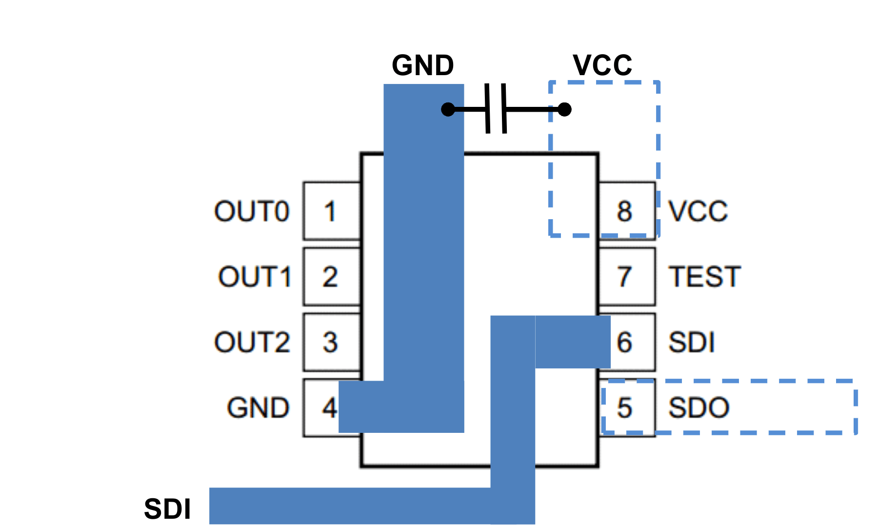
TLC59731 TLC59731-layout.gif Figure 26. Layout Recommendation