SBOS915 December 2017 TLV2172-Q1
PRODUCTION DATA.
- 1 Features
- 2 Applications
- 3 Description
- 4 Revision History
- 5 Pin Configuration and Functions
- 6 Specifications
- 7 Detailed Description
- 8 Application and Implementation
- 9 Power Supply Recommendations
- 10Layout
- 11Device and Documentation Support
- 12Mechanical, Packaging, and Orderable Information
Package Options
Mechanical Data (Package|Pins)
- DGK|8
Thermal pad, mechanical data (Package|Pins)
Orderable Information
6 Specifications
6.1 Absolute Maximum Ratings
over operating free-air temperature range (unless otherwise noted)(1)| MIN | MAX | UNIT | |||
|---|---|---|---|---|---|
| Voltage | Supply voltage, V+ to V− | –20 | 20 | V | |
| Single-supply voltage | 40 | ||||
| Signal input pin(2) | Common-mode | (V–) – 0.5 | (V+) + 0.5 | ||
| Differential(3) | –0.5 | 0.5 | |||
| Current | Signal input pin | –10 | 10 | mA | |
| Output short-circuit(4) | Continuous | ||||
| Operating, TA | –55 | 150 | °C | ||
| Junction, TJ | 150 | ||||
| Storage, Tstg | –65 | 150 | |||
(1) Stresses beyond those listed under Absolute Maximum Ratings may cause permanent damage to the device. These are stress ratings only, which do not imply functional operation of the device at these or any other conditions beyond those indicated under Recommended Operating Conditions. Exposure to absolute-maximum-rated conditions for extended periods may affect device reliability.
(2) Transient conditions that exceed these voltage ratings must be current limited to 10 mA or less.
(3) See the Electrical Overstress section for more information.
(4) Short-circuit to ground, one amplifier per package.
6.2 ESD Ratings
| VALUE | UNIT | |||
|---|---|---|---|---|
| V(ESD) | Electrostatic discharge | Human-body model (HBM), per AEC Q100-002(1) | ±4000 | V |
| Charged-device model (CDM), per AEC Q100-011 | ±1000 | |||
(1) AEC Q100-002 indicates that HBM stressing shall be in accordance with the ANSI/ESDA/JEDEC JS-001 specification.
6.3 Recommended Operating Conditions
over operating free-air temperature range (unless otherwise noted)| MIN | NOM | MAX | UNIT | ||
|---|---|---|---|---|---|
| Supply voltage, (V+) – (V–) | Single-supply | 4.5 | 36 | V | |
| Dual-supply | ±2.25 | ±18 | |||
| Specified temperature | –40 | 125 | °C | ||
6.4 Thermal Information: TLV2172-Q1
| THERMAL METRIC(1) | TLV2172-Q1 | UNIT | ||
|---|---|---|---|---|
| D (SOIC) | DGK (VSSOP) | |||
| 8 PINS | 8 PINS | |||
| RθJA | Junction-to-ambient thermal resistance | 116.1 | 158 | °C/W |
| RθJC(top) | Junction-to-case (top) thermal resistance | 69.8 | 48.6 | °C/W |
| RθJB | Junction-to-board thermal resistance | 56.6 | 78.7 | °C/W |
| ψJT | Junction-to-top characterization parameter | 22.5 | 3.9 | °C/W |
| ψJB | Junction-to-board characterization parameter | 56.1 | 77.3 | °C/W |
| RθJC(bot) | Junction-to-case (bottom) thermal resistance | — | — | °C/W |
(1) For more information about traditional and new thermal metrics, see the Semiconductor and IC Package Thermal Metrics application report.
6.5 Electrical Characteristics
at TA = 25°C, VS = ±2.25 V to ±18 V, VCM = VOUT = VS / 2, and RL = 10 kΩ connected to VS / 2 (unless otherwise noted)| PARAMETER | TEST CONDITIONS | MIN | TYP | MAX | UNIT | ||
|---|---|---|---|---|---|---|---|
| OFFSET VOLTAGE | |||||||
| VOS | Input offset voltage | TA = 25°C | 0.5 | 1.7 | mV | ||
| TA = –40°C to +125°C | 2 | ||||||
| dVOS/dT | Input offset voltage drift | TA = –40°C to +125°C | 1 | µV/°C | |||
| PSRR | Power-supply rejection ratio | VS = 4 V to 36 V, TA = –40°C to +125°C | 100 | 120 | dB | ||
| Channel separation, DC | 5 | µV/V | |||||
| INPUT BIAS CURRENT | |||||||
| IB | Input bias current | TA = 25°C | ±10 | pA | |||
| IOS | Input offset current | TA = 25°C | ±2 | pA | |||
| NOISE | |||||||
| Input voltage noise | f = 0.1 Hz to 10 Hz | 2.5 | µVPP | ||||
| en | Input voltage noise density | f = 100 Hz | 14 | nV/√Hz | |||
| f = 1 kHz | 9 | nV/√Hz | |||||
| in | Input current noise density | f = 1 kHz | 1.6 | fA/√Hz | |||
| INPUT VOLTAGE | |||||||
| VCM | Common-mode voltage range(1) | (V–) – 0.1 | (V+) – 2 | V | |||
| CMRR | Common-mode rejection ratio | VS = ±18 V, (V–) – 0.1 V < VCM < (V+) – 2 V TA = –40°C to +125°C |
94 | 116 | dB | ||
| INPUT IMPEDANCE | |||||||
| Differential | 100 || 4 | MΩ || pF | |||||
| Common-mode | 6 || 4 | 1013 Ω || pF | |||||
| OPEN-LOOP GAIN | |||||||
| AOL | Open-loop voltage gain | (V–) + 0.35 V < VO < (V+) – 0.35 V, TA = –40°C to +125°C | 97 | 115 | dB | ||
| (V–) + 0.5 V < VO < (V+) – 0.5 V, RL = 2 kΩ, TA = –40°C to +125°C |
107 | ||||||
| FREQUENCY RESPONSE | |||||||
| GBP | Gain bandwidth product | 10 | MHz | ||||
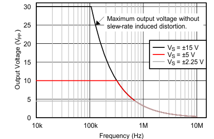
| SR | Slew rate | G = +1 | 10 | V/µs | |||
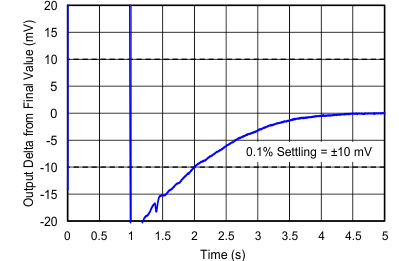
| tS | Settling time | To 0.1%, VS = ±18 V, G = 1, 10-V step | 2 | µs | |||
| To 0.01% (12-bit), VS = ±18 V, G = +1, 10-V step | 3.2 | ||||||
| Overload recovery time | VIN × gain > VS | 200 | ns | ||||
| THD+N | Total harmonic distortion + noise | VS = 36 V, G = +1, f = 1 kHz, VO = 3.5 VRMS | 0.0002% | ||||
| OUTPUT | |||||||
| VO | Voltage output swing from rail | VS = ±18 V, RL = 10 kΩ | TA = 25°C | 70 | mV | ||
| TA = –40°C to +125°C | 95 | ||||||
| VS = ±18 V, RL = 2 kΩ | TA = 25°C | 330 | 400 | ||||
| TA = –40°C to +125°C | 470 | 530 | |||||
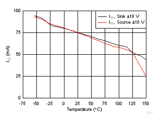
| ISC | Short-circuit current | ±75 | mA | ||||
| CLOAD | Capacitive load drive | See Typical Characteristics | pF | ||||
| RO | Open-loop output resistance | f = 1 MHz, IO = 0 A | 60 | Ω | |||
| POWER SUPPLY | |||||||
| VS | Specified voltage range | 4.5 | 36 | V | |||
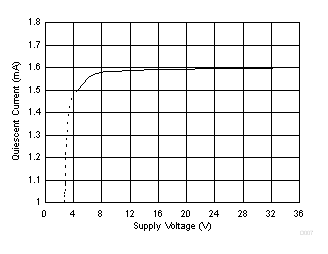
| IQ | Quiescent current per amplifier | IO = 0 A, TA = –40°C to +125°C | 1.6 | 2.3 | mA | ||
(1) The input range can be extended beyond (V+) – 2 V up to V+. See the Typical Characteristics and Application and Implementation sections for additional information.
6.6 Typical Characteristics
at VS = ±18 V, VCM = VS / 2, RLOAD = 10 kΩ connected to VS / 2, and CL = 100 pF (unless otherwise noted)Table 1. Characteristic Performance Measurements
| DESCRIPTION | FIGURE |
|---|---|
| Offset Voltage Production Distribution | Figure 1 |
| Offset Voltage vs Common-Mode Voltage | Figure 2 |
| Offset Voltage vs Common-Mode Voltage (Upper Stage) | Figure 3 |
| Input Bias Current vs Temperature | Figure 4 |
| Output Voltage Swing vs Output Current (Maximum Supply) | Figure 5 |
| CMRR and PSRR vs Frequency (Referred-to-Input) | Figure 6 |
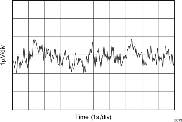
| 0.1-Hz to 10-Hz Noise | Figure 7 |
| Input Voltage Noise Spectral Density vs Frequency | Figure 8 |
| Quiescent Current vs Supply Voltage | Figure 9 |
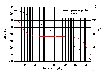
| Open-Loop Gain and Phase vs Frequency | Figure 10 |
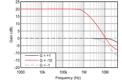
| Closed-Loop Gain vs Frequency | Figure 11 |
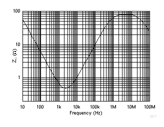
| Open-Loop Output Impedance vs Frequency | Figure 12 |
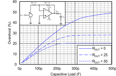
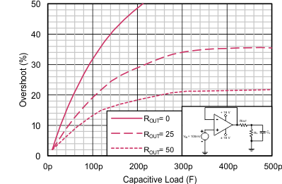
| Small-Signal Overshoot vs Capacitive Load | Figure 13, Figure 14 |
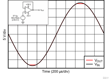
| No Phase Reversal | Figure 15 |
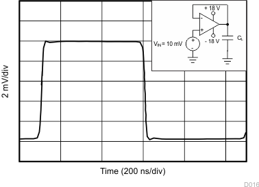
| Small-Signal Step Response (10 mV) | Figure 16, Figure 17 |
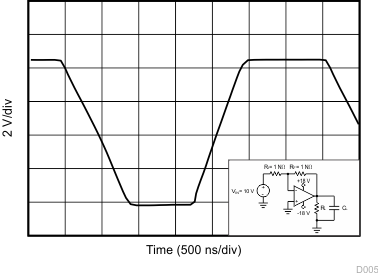
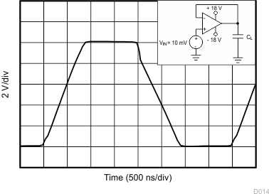
| Large-Signal Step Response | Figure 18, Figure 19 |
| Large-Signal Settling Time | Figure 20, Figure 21 |
| Short-Circuit Current vs Temperature | Figure 22 |
| Maximum Output Voltage vs Frequency | Figure 23 |
| EMIRR IN+ vs Frequency | Figure 24 |
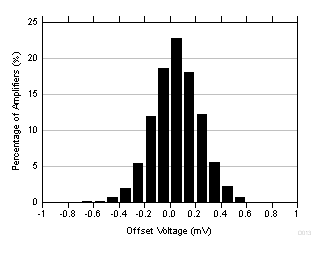
| Distribution taken from 5185 amplifiers |
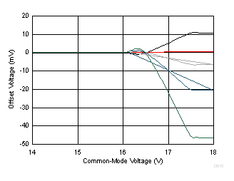
| 5 typical units shown, VS = ±18 V |
(Upper Stage)
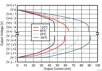
| 100-mV output step, G = –1 | ||
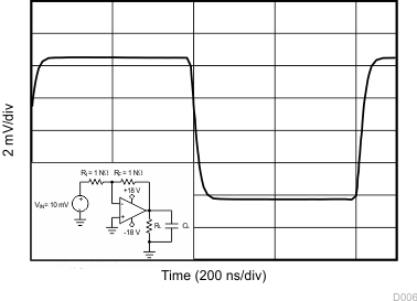
| RL = 1 kΩ | CL = 10 pF | 10-mV step |
| RL = 1 kΩ | CL = 10 pF |
| 10-V negative step | G = 1 | CL = 10 pF |
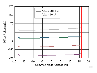
| 5 typical units shown, VS = ±18 V |
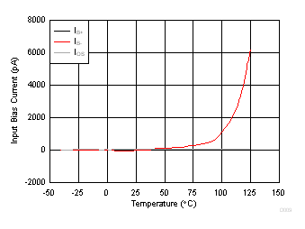
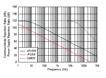
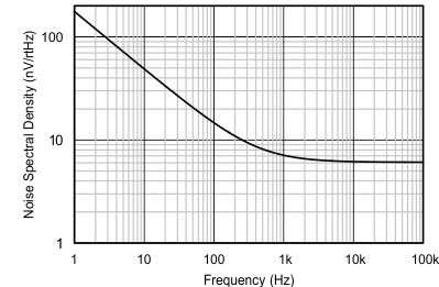
| CLOAD = 15 pF |
| 100-mV output step, G = 1 | ||
| CL = 10 pF | 10-mV step |
| CL = 10 pF |
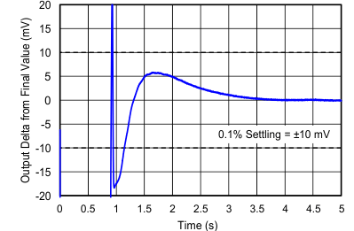
| 10-V positive step | G = 1 | CL = 10 pF |
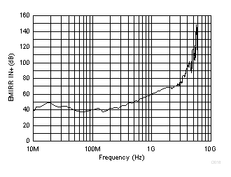
| PRF = –10 dBm | VSUPPLY = ±18 V | VCM = 0 V |