SLOS922A September 2015 – December 2015 TLV27L2-Q1
PRODUCTION DATA.
- 1 Features
- 2 Applications
- 3 Description
- 4 Revision History
- 5 Selection Guide
- 6 Pin Configuration and Functions
- 7 Specifications
- 8 Detailed Description
- 9 Application and Implementation
- 10Power Supply Recommendations
- 11Layout
- 12Device and Documentation Support
- 13Mechanical, Packaging, and Orderable Information
Package Options
Mechanical Data (Package|Pins)
- D|8
Thermal pad, mechanical data (Package|Pins)
Orderable Information
11 Layout
11.1 Layout Guidelines
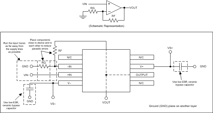
To achieve the levels of high performance of the TLV27L2-Q1 device, follow proper printed-circuit board design techniques. The following list is a general set of guidelines:
- Ground planes—Using a ground plane on the board is highly recommended to provide all components with a low inductive-ground connection. However, in the areas of the amplifier inputs and output, the ground plane can be removed to minimize the stray capacitance.
- Proper power supply decoupling—Use a 6.8-µF tantalum capacitor in parallel with a 0.1-µF ceramic capacitor on each supply terminal. Sharing the tantalum capacitor among several amplifiers is possible depending on the application, but a 0.1-µF ceramic capacitor should always be used on the supply terminal of every amplifier. In addition, the 0.1-µF capacitor should be placed as close as possible to the supply terminal. As this distance increases, the inductance in the connecting trace makes the capacitor less effective. The designer should strive for distances of less than 0.1 inches between the device power terminals and the ceramic capacitors.
- Sockets—Sockets can be used but are not recommended. The additional lead inductance in the socket pins will often lead to stability problems. Surface-mount packages soldered directly to the printed-circuit board are the best implementation.
- Short trace runs and compact part placements—Optimum high performance is achieved when stray series inductance has been minimized. To achieve this performance, the circuit layout should be as compact as possible, thereby minimizing the length of all trace runs. Particular attention should be paid to the inverting input of the amplifier. The length should be kept as short as possible which helps minimize stray capacitance at the input of the amplifier.
- Surface-mount passive components—Using surface-mount passive components is recommended for high performance amplifier circuits for several reasons. First, because of the extremely low lead inductance of surface-mount components, the problem with stray series inductance is greatly reduced. Second, the small size of surface-mount components naturally leads to a more compact layout thereby minimizing both stray inductance and capacitance. If leaded components are used, keep the lead lengths as short as possible.
11.2 Layout Example
 Figure 30. TLV27L2-Q1 Layout Example
11.3 General Power Dissipation Considerations
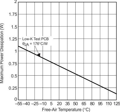
Use to calculate the maximum power dissipation for a given θJA.

where
- PD = Maximum power dissipation of TLV27L2-Q1 IC (watts)
- TMAX = Absolute maximum junction temperature (150°C)
- TA = Free-ambient air temperature (°C)
- θJA = θJC + θCA
- θJC = Thermal coefficient from junction to case
- θCA = Thermal coefficient from case to ambient air (°C/W)

| TJ = 150°C | |||
| Results are with no air flow and using JEDEC Standard Low-K test PCB. | |||