SLAS510G March   2007  – February 2021 TLV320AIC3104

PRODUCTION DATA  

  1. Features
  2. Applications
  3. Description
  4. Revision History
  5. Description (Continued)
  6. Device Comparison Table
  7. Pin Configuration and Functions
  8. Specifications
    1. 8.1 Absolute Maximum Ratings
    2. 8.2 ESD Ratings
    3. 8.3 Recommended Operating Conditions
    4. 8.4 Thermal Information
    5. 8.5 Electrical Characteristics
    6. 8.6 Audio Data Serial Interface Timing Requirements
    7. 8.7 Timing Diagrams
    8. 8.8 Typical Characteristics
  9. Parameter Measurement Information
  10. 10Detailed Description
    1. 10.1 Overview
    2. 10.2 Functional Block Diagrams
    3. 10.3 Feature Description
      1. 10.3.1  Hardware Reset
      2. 10.3.2  Digital Audio Data Serial Interface
        1. 10.3.2.1 Right-Justified Mode
        2. 10.3.2.2 Left-Justified Mode
        3. 10.3.2.3 I2S Mode
        4. 10.3.2.4 DSP Mode
        5. 10.3.2.5 TDM Data Transfer
      3. 10.3.3  Audio Data Converters
        1. 10.3.3.1 Audio Clock Generation
        2. 10.3.3.2 Stereo Audio ADC
          1. 10.3.3.2.1 Stereo Audio ADC High-Pass Filter
          2. 10.3.3.2.2 Automatic Gain Control (AGC)
            1. 10.3.3.2.2.1 Target Level
            2. 10.3.3.2.2.2 Attack Time
            3. 10.3.3.2.2.3 Decay Time
            4. 10.3.3.2.2.4 Noise Gate Threshold
            5. 10.3.3.2.2.5 Maximum PGA Gain Applicable
      4. 10.3.4  Stereo Audio DAC
        1. 10.3.4.1 Digital Audio Processing for Playback
        2. 10.3.4.2 Digital Interpolation Filter
        3. 10.3.4.3 Delta-Sigma Audio DAC
        4. 10.3.4.4 Audio DAC Digital Volume Control
        5. 10.3.4.5 Increasing DAC Dynamic Range
        6. 10.3.4.6 Analog Output Common-Mode Adjustment
        7. 10.3.4.7 Audio DAC Power Control
      5. 10.3.5  Audio Analog Inputs
      6. 10.3.6  Analog Fully Differential Line Output Drivers
      7. 10.3.7  Analog High-Power Output Drivers
      8. 10.3.8  Input Impedance and VCM Control
      9. 10.3.9  MICBIAS Generation
      10. 10.3.10 Short-Circuit Output Protection
      11. 10.3.11 Jack and Headset Detection
    4. 10.4 Device Functional Modes
      1. 10.4.1 Bypass Path Mode
        1. 10.4.1.1 ADC PGA Signal Bypass Path Functionality
        2. 10.4.1.2 Passive Analog Bypass During Power Down
      2. 10.4.2 Digital Audio Processing for Record Path
    5. 10.5 Programming
      1. 10.5.1 I2C Control Interface
        1. 10.5.1.1 I2C Bus Debug in a Glitched System
      2. 10.5.2 Register Map Structure
    6. 10.6 Register Maps
      1. 10.6.1 Output Stage Volume Controls
  11. 11Application and Implementation
    1. 11.1 Application Information
    2. 11.2 Typical Applications
      1. 11.2.1 Typical Connections With Headphone and External Speaker Driver in Portable Application
        1. 11.2.1.1 Design Requirements
        2. 11.2.1.2 Detailed Design Procedure
        3. 11.2.1.3 Application Curves
      2. 11.2.2 Typical Connections for AC-Coupled Headphone Output With Separate Line Outputs and External Speaker Amplifier
        1. 11.2.2.1 Design Requirements
        2. 11.2.2.2 Detailed Design Procedure
        3. 11.2.2.3 Application Curves
  12. 12Power Supply Recommendations
  13. 13Layout
    1. 13.1 Layout Guidelines
    2. 13.2 Layout Example
  14. 14Device and Documentation Support
    1. 14.1 Receiving Notification of Documentation Updates
    2. 14.2 Support Resources
    3. 14.3 Trademarks
    4. 14.4 Electrostatic Discharge Caution
    5. 14.5 Glossary

Package Options

Refer to the PDF data sheet for device specific package drawings

Mechanical Data (Package|Pins)
  • RHB|32
Thermal pad, mechanical data (Package|Pins)
Orderable Information
Maximum PGA Gain Applicable

Allows the user to restrict the maximum PGA gain that can be applied by the AGC algorithm. This can be used for limiting PGA gain in situations where environmental noise is greater than programmed noise threshold. It can be programmed from 0 dB to 59.5 dB in steps of 0.5 dB.
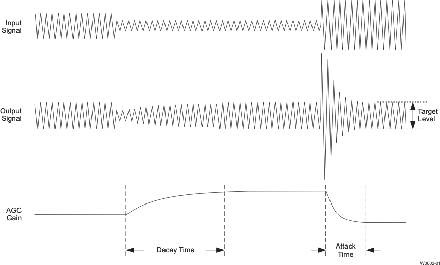
GUID-C0928B4F-A33F-48DF-BC6D-711F3CC17F2E-low.gif Figure 10-9 Typical Operation of the AGC Algorithm During Speech Recording

The time constants here are correct when the ADC is not in double-rate audio mode. The time constants are achieved using the fS(ref) value programmed in the control registers. However, if the fS(ref) is set in the registers to, for example, 48 kHz, but the actual audio clock or PLL programming actually results in a different fS(ref) in practice, then the time constants would not be correct.

The actual AGC decay time maximum is based on a counter length, so the maximum decay time scales with the clock setup that is used. Table 10-2 shows the relationship of the NCODEC ratio to the maximum time available for the AGC decay. In practice, these maximum times are extremely long for audio applications and should not limit any practical AGC decay time that is needed by the system.