SLOS602E September 2008 – September 2019 TLV320AIC3204
PRODUCTION DATA.
- 1 Features
- 2 Applications
- 3 Description
- 4 Revision History
- 5 Device Comparison Table
- 6 Pin Configuration and Functions
-
7 Specifications
- 7.1 Absolute Maximum Ratings
- 7.2 ESD Ratings
- 7.3 Recommended Operating Conditions
- 7.4 Thermal Information
- 7.5 Electrical Characteristics, ADC
- 7.6 Electrical Characteristics, Bypass Outputs
- 7.7 Electrical Characteristics, Microphone Interface
- 7.8 Electrical Characteristics, Audio DAC Outputs
- 7.9 Electrical Characteristics, LDO
- 7.10 Electrical Characteristics, Misc.
- 7.11 Electrical Characteristics, Logic Levels
- 7.12 I2S LJF and RJF Timing in Master Mode (see )
- 7.13 I2S LJF and RJF Timing in Slave Mode (see )
- 7.14 DSP Timing in Master Mode (see )
- 7.15 DSP Timing in Slave Mode (see )
- 7.16 Digital Microphone PDM Timing (see )
- 7.17 I2C Interface Timing
- 7.18 SPI Interface Timing (See )
- 7.19 Typical Characteristics
- 7.20 Typical Characteristics, FFT
- 8 Parameter Measurement Information
- 9 Detailed Description
- 10Application and Implementation
- 11Power Supply Recommendations
- 12Layout
- 13Device and Documentation Support
- 14Mechanical, Packaging, and Orderable Information
Package Options
Mechanical Data (Package|Pins)
- RHB|32
Thermal pad, mechanical data (Package|Pins)
- RHB|32
Orderable Information
7.20 Typical Characteristics, FFT
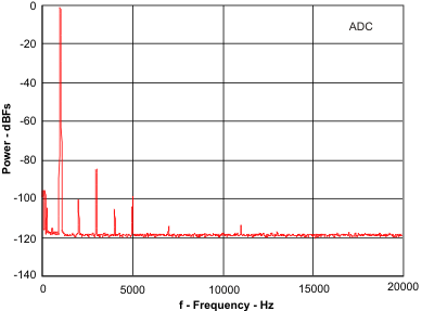 Figure 15. Single Ended Line Input to ADC FFT at -1dBr vs Frequency
 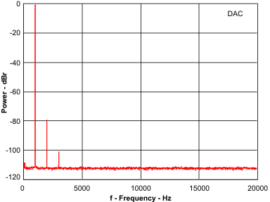 Figure 17. DAC Playback to Line-out FFT at -1dBFS vs Frequency
 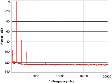 Figure 19. Line Input to Line-out FFT at 446mVrms vs Frequency
 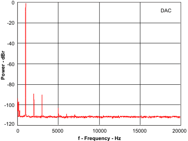 Figure 16. DAC Playback to Headphone FFT at -1dBFS vs Frequency
 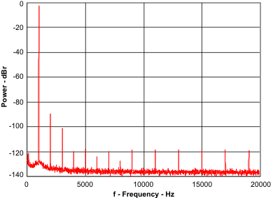 Figure 18. Line Input to Headphone FFT at 446mVrms vs Frequency