SBOS756 October 2016 TLV3541 , TLV3542 , TLV3544
PRODUCTION DATA.
- 1 Features
- 2 Applications
- 3 Description
- 4 Revision History
- 5 Pin Configuration and Functions
- 6 Specifications
- 7 Detailed Description
- 8 Application and Implementation
- 9 Power Supply Recommendations
- 10Layout
- 11Device and Documentation Support
- 12Mechanical, Packaging, and Orderable Information
Package Options
Mechanical Data (Package|Pins)
Thermal pad, mechanical data (Package|Pins)
- D|8
Orderable Information
7 Detailed Description
7.1 Overview
The TLV354x is a CMOS, rail-to-rail I/O, high-speed, voltage-feedback operational amplifier designed for video, high-speed, and other applications. The device is available as a single, dual, or quad op amp.
The amplifier features a 100-MHz gain bandwidth and a 150-V/μs slew rate, but the amplifier is unity-gain stable and operates as a +1-V/V voltage follower.
7.2 Functional Block Diagram
7.3 Feature Description
7.3.1 Operating Voltage
The TLV354x is specified over a power-supply range of 2.7 V to 5.5 V (±1.35 V to ±2.75 V). However, the supply voltage may range from 2.5 V to 5.5 V (±1.25 V to ±2.75 V). Supply voltages higher than 7.5 V (absolute maximum) can permanently damage the amplifier.
Parameters that vary over supply voltage or temperature are shown in the Typical Characteristics section.
7.3.2 Rail-to-Rail Input
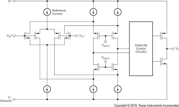
The specified input common-mode voltage range of the TLV354x extends 100 mV beyond the supply rails. This extended range is achieved with a complementary input stage: an N-channel input differential pair in parallel with a P-channel differential pair, as shown in the Functional Block Diagram. The N-channel pair is active for input voltages close to the positive rail, typically (V+) − 1.2 V to 100 mV above the positive supply, while the P-channel pair is on for inputs from 100 mV below the negative supply to approximately (V+) − 1.2 V. There is a small transition region, typically (V+) − 1.5 V to (V+) − 0.9 V, in which both pairs are on. This 600-mV transition region can vary ±500 mV with process variation. Thus, the transition region ( with both input stages on) can range from (V+) − 2.0 V to (V+) − 1.5 V on the low end, up to (V+) − 0.9 V to (V+) − 0.4 V on the high end.
A double-folded cascode adds the signal from the two input pairs and presents a differential signal to the class AB output stage.
7.3.3 Rail-to-Rail Output
A class AB output stage with common-source transistors is used to achieve rail-to-rail output. For high-impedance loads (> 200 Ω), the output voltage swing is typically 100 mV from the supply rails. With 10-Ω loads, a useful output swing can be achieved while maintaining high open-loop gain. See the typical characteristic curves, Output Voltage Swing vs Output Current (Figure 14 and Figure 15).
7.3.4 Output Drive
The TLV354x output stage can supply a continuous output current of ±100 mA and yet provide approximately 2.7 V of output swing on a 5-V supply, as shown in Figure 21. For maximum reliability, it is not recommended to run a continuous DC current in excess of ±100 mA. Refer to the typical characteristic curves, Output Voltage Swing vs Output Current (Figure 14 and Figure 15). For supplying continuous output currents greater than ±100 mA, the TLV354x may be operated in parallel, as shown in Figure 22.
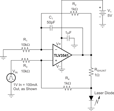 Figure 21. Laser Diode Driver
The TLV354x provides peak currents up to 200 mA, which corresponds to the typical short-circuit current. Therefore, an on-chip thermal shutdown circuit is provided to protect the TLV354x from dangerously high junction temperatures. At 160°C, the protection circuit shuts down the amplifier. Normal operation resumes when the junction temperature cools to below +140°C.
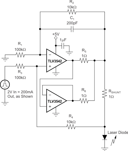 Figure 22. Parallel Operation
7.3.5 Video
The TLV354x output stage is capable of driving standard back-terminated 75-Ω video cables, as shown in Figure 23. By back-terminating a transmission line, the device does not exhibit a capacitive load to its driver. A properly back-terminated 75-Ω cable does not appear as capacitance; the device presents a 150-Ω resistive load to the TLV354x output.
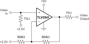 Figure 23. Single-Supply Video Line Driver
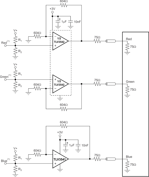
The TLV3542 can be used as an amplifier for RGB graphic signals, which have a voltage of zero at the video black level, by offsetting and AC-coupling the signal. See Figure 24.
7.3.6 Driving Analog-to-Digital Converters
The TLV354x series op amps offer 60 ns of settling time to 0.01%, making them a good choice for driving high- and medium-speed sampling A/D converters and buffering reference circuits. The TLV354x series provide an effective means of buffering the A/D converter input capacitance and resulting charge injection while providing signal gain. For applications requiring high DC accuracy, TI recommends using the OPA350 series.
Figure 25 illustrates the TLV3541 driving an A/D converter. With the TLV3541 in an inverting configuration, a capacitor across the feedback resistor can filter high-frequency noise in the signal.
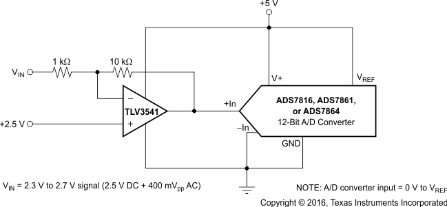 Figure 25. The TLV3541 in Inverting Configuration Driving the ADS7816
7.3.7 Capacitive Load and Stability
The TLV354x series op amps can drive a wide range of capacitive loads. However, all op amps under certain conditions may become unstable. Op amp configuration, gain, and load value are just a few of the factors to consider when determining stability. An op amp in unity-gain configuration is most susceptible to the effects of capacitive loading. The capacitive load reacts with the device output resistance, along with any additional load resistance, to create a pole in the small-signal response that degrades the phase margin. Refer to the typical characteristic curve, Frequency Response for Various CL (Figure 7) for details.
The TLV354x topology enhances the ability to drive capacitive loads. In unity gain, these op amps perform well with large capacitive loads. Refer to the typical characteristic curves, Recommended RS vs Capacitive Load (Figure 8) and Frequency Response vs Capacitive Load (Figure 9) for details.
One method of improving capacitive load drive in the unity-gain configuration is to insert a 10-Ω to 20-Ω resistor in series with the output, as shown in Figure 26. This configuration significantly reduces ringing with large capacitive loads. See the typical characteristic curve, Frequency Response vs Capacitive Load (Figure 9). However, if there is a resistive load in parallel with the capacitive load, RS creates a voltage divider. This voltage division introduces a DC error at the output and slightly reduces output swing. This error may be insignificant. For instance, with RL = 10 kΩ and RS = 20 Ω, there is an error of approximately 0.2% at the output.
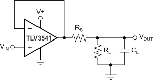 Figure 26. Series Resistor in Unity-Gain Configuration Improves Capacitive Load Drive
7.3.8 Wideband Transimpedance Amplifier
Wide bandwidth, low input bias current, and low input voltage and current noise make the TLV354x a suitable wideband photodiode transimpedance amplifier for low-voltage, single-supply applications. Low-voltage noise is important because photodiode capacitance causes the effective noise gain of the circuit to increase at high frequency.
The key elements to a transimpedance design, as shown in Figure 27, are the expected diode capacitance (including the parasitic input common-mode and differential-mode input capacitance (2 + 2) pF for the TLV354x), the desired transimpedance gain (RF), and the Gain-Bandwidth Product (GBW) for the TLV354x (100 MHz, typical). With these three variables set, the feedback capacitor value (CF) may be set to control the frequency response.
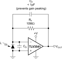 Figure 27. Transimpedance Amplifier
To achieve a flat, second-order, Butterworth frequency response, the feedback pole must be set as shown in Equation 1:

Typical surface-mount resistors have a parasitic capacitance of approximately 0.2 pF that must be deducted from the calculated feedback capacitance value. Bandwidth is calculated by Equation 2:

For even higher transimpedance bandwidth, the high-speed CMOS OPA355 (200-MHz GBW) or the OPA655 (400-MHz GBW) may be used.
7.4 Device Functional Modes
The TLV354x has dual functional modes and is operational when the power-supply voltage is greater than 2.5 V (±1.25 V). The maximum power-supply voltage for the TLV354x is 5.5 V (±2.75 V). At +160°C, the protection circuit shuts down the amplifier. Normal operation resumes when the junction temperature cools to below +140°C.