SNVSB04C March 2019 – December 2021 TLV4021 , TLV4031 , TLV4041 , TLV4051
PRODUCTION DATA
- 1 Features
- 2 Applications
- 3 Description
- 4 Revision History
- 5 Pin Configuration and Functions
- 6 Specifications
- 7 Typical Characteristics
- 8 Detailed Description
- 9 Application and Implementation
- 10Power Supply Recommendations
- 11Layout
- 12Device and Documentation Support
- 13Mechanical, Packaging, and Orderable Information
Package Options
Mechanical Data (Package|Pins)
- YKA|4
Thermal pad, mechanical data (Package|Pins)
Orderable Information
8.4.3 Switching Thresholds and Hysteresis (VHYS)
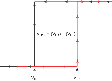
The TLV40x1 transfer curve is shown in Figure 8-5.
- VIT+ represents the positive-going input threshold that causes the comparator output to change from a logic low state to a logic high state.
- VIT- represents the negative-going input threshold that causes the comparator output to change from a logic high state to a logic low state.
- VHYS represents the difference between VIT+ and VIT- and is 20 mV for TLV40x1Ry and 54 mV for TLV4021S5x.
 Figure 8-5 Transfer Curve
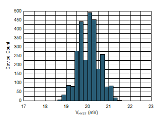
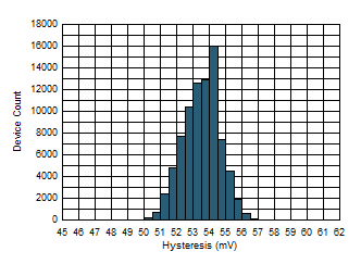
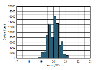
VIT+ and VIT- have mV's of variation over temperature. The significant portion of the variation of these parameters is a result of the internal bandgap voltage from which VIT+ and VIT- are derived. The following hysteresis histograms demonstrate the performance of the TLV40x1 hysteresis circuitry. Since the bandgap reference is used to set VIT+ and VIT-, each of these parameters have a tendency to error (track) in the same direction. For example, if VIT+ has a positive 0.5% error, VIT- would have a tendency to have a similar positive percentage error. As a result, the variation of hysteresis will never be equal to the difference of the highest VIT+ value of its range and the lowest VIT- value of its range.
 Figure 8-6 VHYST Histogram (TLV40x1R2, VS=5V)
 Figure 8-8 VHYST Histogram (TLV40x1S5, VS=5V)
 Figure 8-7 VHYST Histogram (TLV40x1R1, VS=5V)