SLVSE95B April   2018  – March 2020 TLV62568A , TLV62569A

PRODUCTION DATA.  

  1. Features
  2. Applications
  3. Description
    1.     Device Images
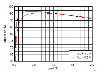
      1.      sp sp spTypical Application Schematic
      2.      sp spEfficiency at 5-V Input Voltage
  4. Revision History
  5. Pin Configuration and Functions
    1.     Pin Functions
  6. Specifications
    1. 6.1 Absolute Maximum Ratings
    2. 6.2 ESD Ratings
    3. 6.3 Recommended Operating Conditions
    4. 6.4 Thermal Information
    5. 6.5 Electrical Characteristics
    6. 6.6 Typical Characteristics
  7. Detailed Description
    1. 7.1 Overview
    2. 7.2 Functional Block Diagrams
    3. 7.3 Feature Description
      1. 7.3.1 100% Duty Cycle Low Dropout Operation
      2. 7.3.2 Soft Startup
      3. 7.3.3 Switch Current Limit
      4. 7.3.4 Under Voltage Lockout
      5. 7.3.5 Thermal Shutdown
    4. 7.4 Device Functional Modes
      1. 7.4.1 Enabling/Disabling the Device
      2. 7.4.2 Power Good
  8. Application and Implementation
    1. 8.1 Application Information
    2. 8.2 Typical Application
      1. 8.2.1 Design Requirements
      2. 8.2.2 Detailed Design Procedure
        1. 8.2.2.1 Custom Design With WEBENCH® Tools
        2. 8.2.2.2 Setting the Output Voltage
        3. 8.2.2.3 Output Filter Design
        4. 8.2.2.4 Inductor Selection
        5. 8.2.2.5 Input and Output Capacitor Selection
      3. 8.2.3 Application Performance Curves
  9. Power Supply Recommendations
  10. 10Layout
    1. 10.1 Layout Guidelines
    2. 10.2 Layout Example
    3. 10.3 Thermal Considerations
  11. 11Device and Documentation Support
    1. 11.1 Device Support
      1. 11.1.1 Third-Party Products Disclaimer
      2. 11.1.2 Development Support
        1. 11.1.2.1 Custom Design With WEBENCH® Tools
    2. 11.2 Documentation Support
      1. 11.2.1 Related Documentation
    3. 11.3 Receiving Notification of Documentation Updates
    4. 11.4 Support Resources
    5. 11.5 Trademarks
    6. 11.6 Electrostatic Discharge Caution
    7. 11.7 Glossary
  12. 12Mechanical, Packaging, and Orderable Information

Package Options

Mechanical Data (Package|Pins)
Thermal pad, mechanical data (Package|Pins)
Orderable Information

Application Performance Curves

VIN = 5 V, VOUT = 1.8 V, TA = 25 °C, external components shown in Table 3, unless otherwise noted.
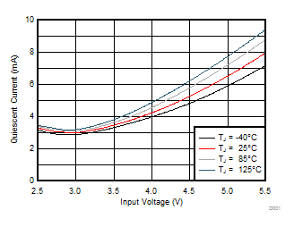
TLV62568A TLV62569A D001-SLVSE95_TLV62569A-01.gif
VOUT = 0.6 V
Figure 7. Quiescent Current
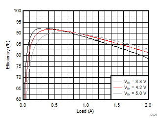
TLV62568A TLV62569A D006-SLVSE95_TLV62569A-01.gif
Figure 9. 1.2-V Output Efficiency
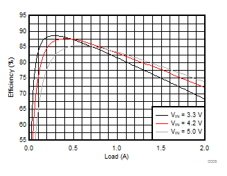
TLV62568A TLV62569A D005-SLVSE95_TLV62569A-01.gif
Figure 8. 0.6-V Output Efficiency
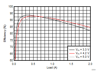
TLV62568A TLV62569A D004-SLVSE95_TLV62569A-01.gif
Figure 10. 1.8-V Output Efficiency
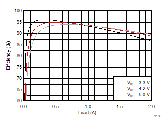
TLV62568A TLV62569A D023-SLVSE95_TLV62569A-01.gif
Figure 11. 2.5-V Output Efficiency
TLV62568A TLV62569A D008-SLVSE95_TLV62569A-01.gif
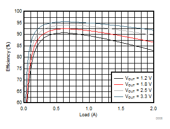
Figure 13. 5.0-V Input Efficiency
TLV62568A TLV62569A D010-SLVSE95_TLV62569A-01.gif
IOUT = 1 A
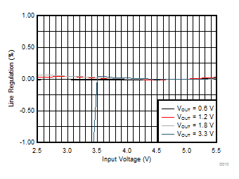
Figure 15. Line Regulation
TLV62568A TLV62569A D011-SLVSE95_TLV62569A-01.gif
VIN = 5 V
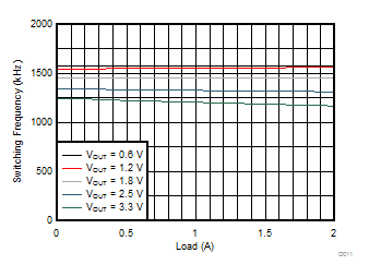
Figure 17. Switching Frequency vs Load
TLV62568A TLV62569A D014-SLVSE95-TLV62569A.gif
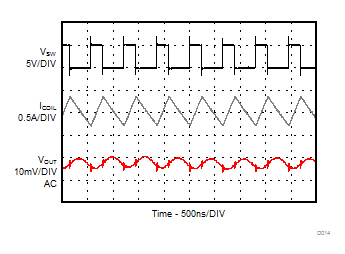
IOUT = 36 mA
Figure 19. PWM Operation
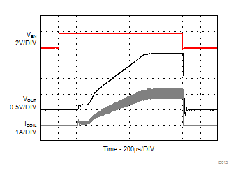
TLV62568A TLV62569A D015-SLVSE95-TLV62569A.gif
Load = 0.9 Ω
Figure 21. Startup and Shutdown with Load
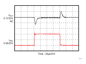
TLV62568A TLV62569A D017-SLVSE95-TLV62569A.gif
Load Step 0 A to 1 A, 1A/μs slew rate
Figure 23. Load Transient
TLV62568A TLV62569A D007-SLVSE95_TLV62569A-01.gif
Figure 12. 3.3-V Output Efficiency
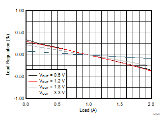
TLV62568A TLV62569A D009-SLVSE95_TLV62569A-01.gif
VIN = 5 V
Figure 14. Load Regulation
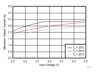
TLV62568A TLV62569A D019-SLVSE95_TLV62569A-01.gif
PG is high
Figure 16. Maximum Output Current at VOUT = 1.8 V
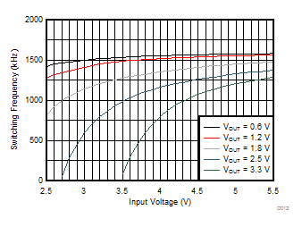
TLV62568A TLV62569A D012-SLVSE95_TLV62569A-01.gif
IOUT = 1 A
Figure 18. Switching Frequency vs Input Voltage
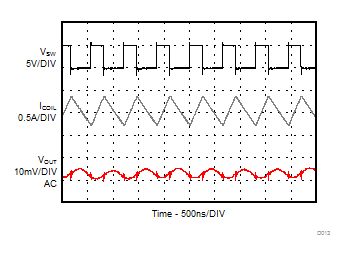
TLV62568A TLV62569A D013-SLVSE95-TLV62569A.gif
IOUT = 1 A
Figure 20. PWM Operation
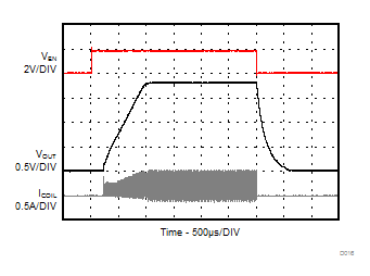
TLV62568A TLV62569A D016-SLVSE95-TLV62569A.gif
Load = 9 Ω
Figure 22. Startup and Shutdown with Load
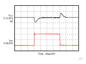
TLV62568A TLV62569A D018-SLVSE95-TLV62569A.gif
Load Step 0 A to 1 A, 1A/μs slew rate C3 = 10 pF
Figure 24. Load Transient with A Feed Forward Capacitor