SBOS865B January   2018  – November 2019 TLV6703

PRODUCTION DATA.  

  1. Features
  2. Applications
  3. Description
    1.     Device Images
      1.      Simplified Block Diagram
  4. Revision History
  5. Device Comparison Table
  6. Pin Configuration and Functions
    1.     Pin Functions
  7. Specifications
    1. 7.1 Absolute Maximum Ratings
    2. 7.2 ESD Ratings
    3. 7.3 Recommended Operating Conditions
    4. 7.4 Thermal Information
    5. 7.5 Electrical Characteristics
    6. 7.6 Timing Requirements
    7. 7.7 Switching Characteristics
    8. 7.8 Typical Characteristics
  8. Detailed Description
    1. 8.1 Overview
    2. 8.2 Functional Block Diagram
    3. 8.3 Feature Description
      1. 8.3.1 Input Pin (SENSE)
      2. 8.3.2 Output Pin (OUT)
      3. 8.3.3 Immunity to Input-Pin Voltage Transients
    4. 8.4 Device Functional Modes
      1. 8.4.1 Normal Operation (VDD > UVLO)
      2. 8.4.2 Undervoltage Lockout (V(POR) < VDD < UVLO)
      3. 8.4.3 Power-On Reset (VDD < V(POR))
  9. Application and Implementation
    1. 9.1 Application Information
      1. 9.1.1 VPULLUP to a Voltage Other Than VDD
      2. 9.1.2 Monitoring VDD
      3. 9.1.3 Monitoring a Voltage Other Than VDD
    2. 9.2 Typical Application
      1. 9.2.1 Design Requirements
      2. 9.2.2 Detailed Design Procedure
        1. 9.2.2.1 Resistor Divider Selection
        2. 9.2.2.2 Pullup Resistor Selection
        3. 9.2.2.3 Input Supply Capacitor
        4. 9.2.2.4 Sense Capacitor
      3. 9.2.3 Application Curves
    3. 9.3 Dos and Don'ts
  10. 10Power-Supply Recommendations
  11. 11Layout
    1. 11.1 Layout Guidelines
    2. 11.2 Layout Example
  12. 12Device and Documentation Support
    1. 12.1 Device Support
      1. 12.1.1 Development Support
    2. 12.2 Receiving Notification of Documentation Updates
    3. 12.3 Community Resources
    4. 12.4 Trademarks
    5. 12.5 Electrostatic Discharge Caution
    6. 12.6 Glossary
  13. 13Mechanical, Packaging, and Orderable Information

Package Options

Mechanical Data (Package|Pins)
Thermal pad, mechanical data (Package|Pins)
Orderable Information

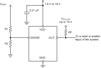
VPULLUP to a Voltage Other Than VDD

The output is often tied to VDD through a resistor. However, some applications may require the output to be pulled up to a higher or lower voltage than VDD to correctly interface with the reset and enable pins of other devices.
TLV6703 typ_app1_sbvs271.gifFigure 14. Interfacing to a Voltage Other Than VDD