SBVS153G february   2011  – june 2023 TLV707 , TLV707P

PRODUCTION DATA  

  1.   1
  2. Features
  3. Applications
  4. Description
  5. Revision History
  6. Pin Configuration and Functions
  7. Specifications
    1. 6.1 Absolute Maximum Ratings
    2. 6.2 ESD Ratings
    3. 6.3 Recommended Operating Conditions
    4. 6.4 Thermal Information
    5. 6.5 Electrical Characteristics
    6. 6.6 Typical Characteristics
  8. Detailed Description
    1. 7.1 Overview
    2. 7.2 Functional Block Diagrams
    3. 7.3 Feature Description
      1. 7.3.1 Internal Current Limit
      2. 7.3.2 Shutdown
    4. 7.4 Device Functional Modes
  9. Application and Implementation
    1. 8.1 Application Information
    2. 8.2 Typical Application
      1. 8.2.1 Design Requirements
      2. 8.2.2 Detailed Design Procedure
        1. 8.2.2.1 Input and Output Capacitor Requirements
        2. 8.2.2.2 Dropout Voltage
        3. 8.2.2.3 Transient Response
      3. 8.2.3 Application Curves
    3. 8.3 Best Design Practices
    4. 8.4 Power Supply Recommendations
    5. 8.5 Layout
      1. 8.5.1 Layout Guidelines
        1. 8.5.1.1 Board Layout Recommendations to Improve PSRR and Noise Performance
        2. 8.5.1.2 Package Mounting
        3. 8.5.1.3 Thermal Considerations
        4. 8.5.1.4 Power Dissipation
      2. 8.5.2 Layout Example
  10. Device and Documentation Support
    1. 9.1 Device Support
      1. 9.1.1 Development Support
        1. 9.1.1.1 Evaluation Modules
        2. 9.1.1.2 Spice Models
      2. 9.1.2 Device Nomenclature
    2. 9.2 Documentation Support
      1. 9.2.1 Related Documentation
    3. 9.3 Receiving Notification of Documentation Updates
    4. 9.4 Support Resources
    5. 9.5 Trademarks
    6. 9.6 Electrostatic Discharge Caution
    7. 9.7 Glossary
  11. 10Mechanical, Packaging, and Orderable Information

Package Options

Mechanical Data (Package|Pins)
Thermal pad, mechanical data (Package|Pins)
Orderable Information

Description

The TLV707 series (TLV707 and TLV707P) of low-dropout linear regulators (LDOs) are low quiescent current devices with excellent line and load transient performance for power-sensitive applications. These devices provide a typical accuracy of 0.5%. All versions have thermal shutdown and overcurrent protection for safety.

Furthermore, these devices are stable with an effective output capacitance of only 0.1 µF. This feature enables the use of cost-effective capacitors that have higher bias voltages and temperature derating. These devices also regulate to the specified accuracy with no output load.

The TLV707P also provides an active pulldown circuit to quickly discharge the outputs.

The TLV707 series of LDOs are available in a 1-mm × 1-mm DQN (X2SON) package that makes them desirable for handheld applications.

Package Information
PART NUMBER PACKAGE(1) PACKAGE SIZE(2)
TLV707 DQN (X2SON, 4) 1.00 mm × 1.00 mm
TLV707P
For all available packages, see the package option addendum at the end of the data sheet.
The package size (length × width) is a nominal value and includes pins, where applicable.


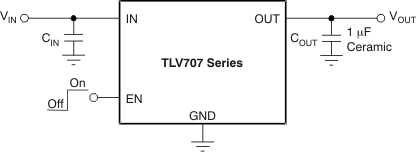
GUID-76361974-104D-4576-895E-9DB6BBBD2271-low.gif Typical Application Circuit