SBVS153G february   2011  – june 2023 TLV707 , TLV707P

PRODUCTION DATA  

  1.   1
  2. Features
  3. Applications
  4. Description
  5. Revision History
  6. Pin Configuration and Functions
  7. Specifications
    1. 6.1 Absolute Maximum Ratings
    2. 6.2 ESD Ratings
    3. 6.3 Recommended Operating Conditions
    4. 6.4 Thermal Information
    5. 6.5 Electrical Characteristics
    6. 6.6 Typical Characteristics
  8. Detailed Description
    1. 7.1 Overview
    2. 7.2 Functional Block Diagrams
    3. 7.3 Feature Description
      1. 7.3.1 Internal Current Limit
      2. 7.3.2 Shutdown
    4. 7.4 Device Functional Modes
  9. Application and Implementation
    1. 8.1 Application Information
    2. 8.2 Typical Application
      1. 8.2.1 Design Requirements
      2. 8.2.2 Detailed Design Procedure
        1. 8.2.2.1 Input and Output Capacitor Requirements
        2. 8.2.2.2 Dropout Voltage
        3. 8.2.2.3 Transient Response
      3. 8.2.3 Application Curves
    3. 8.3 Best Design Practices
    4. 8.4 Power Supply Recommendations
    5. 8.5 Layout
      1. 8.5.1 Layout Guidelines
        1. 8.5.1.1 Board Layout Recommendations to Improve PSRR and Noise Performance
        2. 8.5.1.2 Package Mounting
        3. 8.5.1.3 Thermal Considerations
        4. 8.5.1.4 Power Dissipation
      2. 8.5.2 Layout Example
  10. Device and Documentation Support
    1. 9.1 Device Support
      1. 9.1.1 Development Support
        1. 9.1.1.1 Evaluation Modules
        2. 9.1.1.2 Spice Models
      2. 9.1.2 Device Nomenclature
    2. 9.2 Documentation Support
      1. 9.2.1 Related Documentation
    3. 9.3 Receiving Notification of Documentation Updates
    4. 9.4 Support Resources
    5. 9.5 Trademarks
    6. 9.6 Electrostatic Discharge Caution
    7. 9.7 Glossary
  11. 10Mechanical, Packaging, and Orderable Information

Package Options

Mechanical Data (Package|Pins)
Thermal pad, mechanical data (Package|Pins)
Orderable Information

Shutdown

The enable pin (EN) is active high. The device is enabled when voltage at the EN pin goes above 0.9 V. This relatively lower voltage value required to turn on the LDO can also be used to power the device when connected to a GPIO of a newer processor, where the GPIO logic 1 voltage level is lower than that of traditional microcontrollers. The device is turned off when the EN pin is held at less than 0.4 V. When shutdown capability is not required, EN can be connected to the IN pin.

The TLV707P version has internal active pulldown circuitry that discharges the output with a time constant as given by Equation 1:
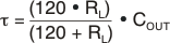
Equation 1. GUID-C7C45BD7-72C8-4726-800C-94AA86F02C4D-low.gif

where:

  • RL = Load resistance
  • COUT = Output capacitor