SLLSEN7E October 2015 – September 2017 TMDS171
PRODUCTION DATA.
- 1 Features
- 2 Applications
- 3 Description
- 4 Revision History
- 5 Pin Configuration and Functions
- 6 Specifications
- 7 Parameter Measurement Information
-
8 Detailed Description
- 8.1 Overview
- 8.2 Functional Block Diagram
- 8.3
Feature Description
- 8.3.1 Reset Implementation
- 8.3.2 Operation Timing
- 8.3.3 Swap and Polarity Working (Retimer Mode Only)
- 8.3.4 TMDS Inputs
- 8.3.5 TMDS Inputs Debug Tools
- 8.3.6 Receiver Equalizer
- 8.3.7 Input Signal Detect Block
- 8.3.8 Audio Return Channel
- 8.3.9 Transmitter Impedance Control
- 8.3.10 TMDS Outputs
- 8.3.11 Pre-Emphasis/De-Emphasis
- 8.4 Device Functional Modes
- 8.5
Register Maps
- 8.5.1 Local I2C Overview
- 8.5.2 CSR Bit Field Definitions, DEVICE_ID (offset: 00000000 ≈ 00000111) (reset:00h ≈ 07h)
- 8.5.3 CSR Bit Field Definitions, REV _ID (offset: 00001000) (reset: 01h)
- 8.5.4 CSR BIT Field Definitions - Misc Control (offset: 00001001) (reset: 02h)
- 8.5.5 CSR BIT Field Definitions - Misc Control (offset: 00001010) (reset: B1h)
- 8.5.6 CSR BIT Field Definitions - Misc Control (offset: 00001011) (reset: 00h)
- 8.5.7 CSR BIT Field Definitions - Misc Control (offset: 00001100) (reset: 00h)
- 8.5.8 CSR BIT Field Definitions - Equalization Control Register (offset: 00001101) (reset: 01h)
- 8.5.9 CSR BIT Field Definitions - RX Pattern Verifier Control/Status (offset: 00001110) (reset: 00h)
- 8.5.10 CSR BIT Field Definitions - RX Pattern Verifier Control/Status (offset: 00001111) (reset: 00h)
- 8.5.11 CSR BIT Field Definitions - RX Pattern Verifier Control/Status (offset: 00010000) (reset: 00h)
- 8.5.12 CSR BIT Field Definitions - RX Pattern Verifier Control/Status (offset: 00010001) (reset: 00h)
- 8.5.13 CSR BIT Field Definitions - RX Pattern Verifier Control/Status (offset: 00010010) (reset: 00h)
- 8.5.14 CSR BIT Field Definitions - RX Pattern Verifier Control/Status (offset: 00010011) (reset: 00h)
- 8.5.15 CSR BIT Field Definitions - RX Pattern Verifier Control/Status (offset: 00010100) (reset: 00h)
- 8.5.16 CSR BIT Field Definitions - RX Pattern Verifier Control/Status (offset: 00010101) (reset: 00h)
- 8.5.17 CSR BIT Field Definitions - RX Pattern Verifier Control/Status (offset: 00010110) (reset: 00h)
- 8.5.18 CSR BIT Field Definitions - RX Pattern Verifier Control/Status (offset: 00010111) (reset: 00h)
- 8.5.19 CSR BIT Field Definitions - RX Pattern Verifier Control/Status (offset: 00011000) (reset: 00h)
- 8.5.20 CSR BIT Field Definitions - RX Pattern Verifier Control/Status (offset: 00011001) (reset: 00h)
- 8.5.21 CSR BIT Field Definitions - RX Pattern Verifier Control/Status (offset: 00011010) (reset: 00h)
- 8.5.22 CSR BIT Field Definitions - RX Pattern Verifier Control/Status (offset: 00011011) (reset: 00h)
- 8.5.23 CSR BIT Field Definitions - RX Pattern Verifier Control/Status (offset: 00011100) (reset: 00h)
- 8.5.24 CSR BIT Field Definitions - RX Pattern Verifier Control/Status (offset: 00011101) (reset: 00h)
- 8.5.25 CSR BIT Field Definitions - RX Pattern Verifier Control/Status (offset: 00011110) (reset: 00h)
- 8.5.26 CSR BIT Field Definitions - RX Pattern Verifier Control/Status (offset: 00011111) (reset: 00h)
- 8.5.27 CSR BIT Field Definitions - RX Pattern Verifier Control/Status (offset: 00100000) (reset: 00h)
- 9 Application and Implementation
- 10Power Supply Recommendations
- 11Layout
- 12Device and Documentation Support
- 13Mechanical, Packaging, and Orderable Information
Package Options
Mechanical Data (Package|Pins)
- RGZ|48
Thermal pad, mechanical data (Package|Pins)
- RGZ|48
Orderable Information
7 Parameter Measurement Information
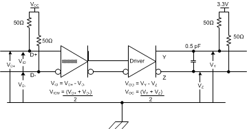 Figure 4. TMDS Main Link Test Circuit
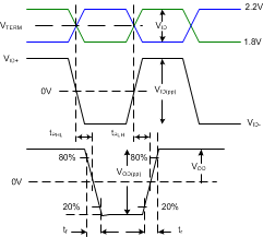 Figure 5. Input/Output Timing Measurements
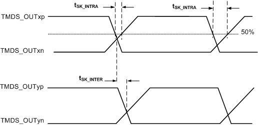 Figure 6. TMDS Output Skew Measurements
 Figure 7. HDMI/DVI TMDS Output Common Mode Measurement
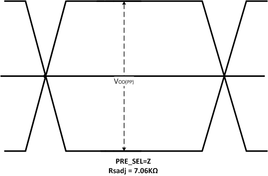 Figure 8. Output Differential Waveform
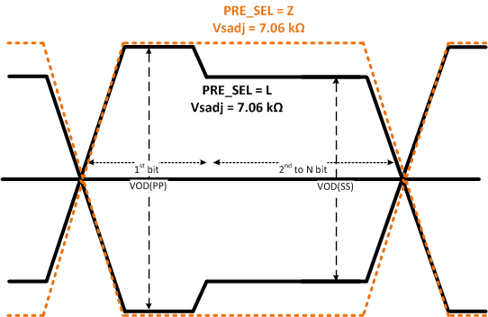 Figure 9. Output De-emphasis Waveform
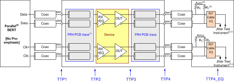
1. The FR4 trace between TTP1 and TTP2 is designed to emulate 1-8” of FR4, connector and another 1-8” of FR4. Trace width – 4 mils. 100 Ω differential impedance.
2. All Jitter is measured at a BER of 10-9
3. Residual jitter reflects the total jitter measured at TTP4 minus the jitter measured at TTP1
4. AVCC = 3.3 V
5. RT = 50 Ω
6. The input signal from parallel Bert does not have any pre-emphasis. Refer to Recommended Operating Conditions.
Figure 10. Jitter Measurement Circuit
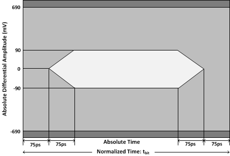 Figure 11. HDMI Output Jitter Measurement
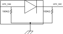 Figure 12. HPD Test Circuit
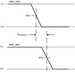 Figure 13. HPD Timing Diagram No. 1
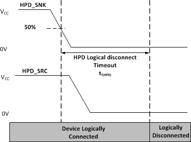 Figure 14. HPD Logic Disconnect Timeout
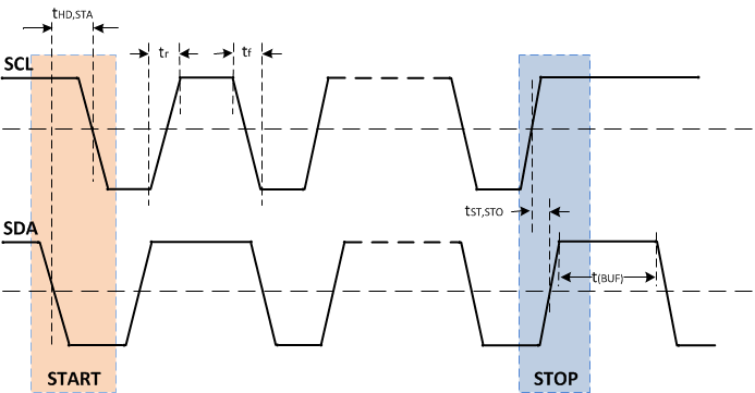 Figure 15. Start and Stop Condition Timing
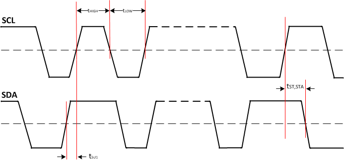 Figure 16. SCL and SDA Timing
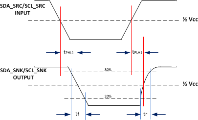 Figure 17. DDC Propagation Delay – Source to Sink
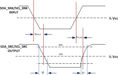 Figure 18. DDC Propagation Delay – Sink to Source
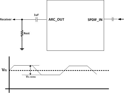 Figure 19. ARC Output
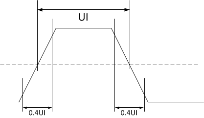 Figure 20. Rise/Fall Time of ARC