SBOS564B November   2011  – December 2018 TMP104

PRODUCTION DATA.  

  1. 1Features
  2. 2Applications
  3. 3Description
    1.     Device Images
      1.      Typical Application
  4. 4Revision History
  5. 5Pin Configuration and Functions
    1.     Pin Functions
  6. 6Specifications
    1. 6.1 Absolute Maximum Ratings
    2. 6.2 ESD Ratings
    3. 6.3 Thermal Information
    4. 6.4 Electrical Characteristics
    5. 6.5 Typical Characteristics
  7. 7Detailed Description
    1. 7.1 Overview
    2. 7.2 Feature Description
      1. 7.2.1 Timeout Function
      2. 7.2.2 Noise
      3. 7.2.3 SMAART Wire™ Interface Timing Specifications
    3. 7.3 Programming
      1. 7.3.1 Communication Protocol
      2. 7.3.2 Command Register
      3. 7.3.3 Global Initialization and Address Assignment Sequence
      4. 7.3.4 Global Read and Write
      5. 7.3.5 Global Clear Interrupt
      6. 7.3.6 Global Software Reset
      7. 7.3.7 Individual Read and Write
    4. 7.4 Register Maps
      1. 7.4.1 Temperature Register
      2. 7.4.2 Configuration Register
        1. 7.4.2.1 Temperature Watchdog Function (FH, FL)
        2. 7.4.2.2 Conversion Rate (CR1, CR0)
        3. 7.4.2.3 Conversion Modes
          1. 7.4.2.3.1 Shutdown Mode (M1 = 0, M0 = 0)
          2. 7.4.2.3.2 One-Shot Mode (M1 = 0, M0 = 1)
          3. 7.4.2.3.3 Continuous Conversion Mode (M1 = 1)
        4. 7.4.2.4 Interrupt Functionality (INT_EN)
      3. 7.4.3 Temperature Limit Registers
  8. 8Device and Documentation Support
    1. 8.1 Receiving Notification of Documentation Updates
    2. 8.2 Community Resources
    3. 8.3 Trademarks
    4. 8.4 Electrostatic Discharge Caution
    5. 8.5 Glossary
  9. 9Mechanical, Packaging, and Orderable Information

Package Options

Refer to the PDF data sheet for device specific package drawings

Mechanical Data (Package|Pins)
  • YFF|4
Thermal pad, mechanical data (Package|Pins)
Orderable Information

Command Register

Figure 8 shows the internal register structure of the TMP104. Communications between the registers are transferred through the interface in LSB-first order. The 8-bit Command Register, as shown in Table 3, is used to determine the type of instruction being addressed. These eight bits could either interpret a global instruction or an individual instruction, which is determined by the value of P7. When P7 = 0, the command byte interprets an individual instruction; when P7 = 1, the command byte interprets a global instruction.
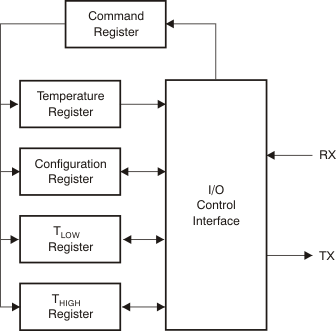
TMP104 ai_internal_register_bos564.gifFigure 8. Internal Register Structure

Table 3. Command Register Byte

P7 P6 P5 P4 P3 P2 P1 P0
GLB IN3/ID3 IN2/ID2 IN1/ID1 IN0/ID0 P1 P0 R/W