SNIS216 November   2019 TMP392

PRODUCTION DATA.  

  1. Features
  2. Applications
  3. Description
    1.     Simplified Schematic
  4. Revision History
  5. Pin Configuration and Functions
    1.     Pin Functions
  6. Specifications
    1. 6.1 Absolute Maximum Ratings
    2. 6.2 ESD Ratings
    3. 6.3 Recommended Operating Conditions
    4. 6.4 Thermal Information
    5. 6.5 Electrical Characteristics
    6. 6.6 Typical Characteristics
  7. Detailed Description
    1. 7.1 Overview
    2. 7.2 Functional Block Diagram
    3. 7.3 Feature Description
      1. 7.3.1 TMP392 Programming Tables
      2. 7.3.2 Trip Test
      3. 7.3.3 20°C Hysteresis
    4. 7.4 Device Functional Modes
  8. Application and Implementation
    1. 8.1 Applications Information
    2. 8.2 Typical Applications
      1. 8.2.1 Simplified Application Schematic
        1. 8.2.1.1 Design Requirements
        2. 8.2.1.2 Detailed Design Procedure
        3. 8.2.1.3 Application Curves
      2. 8.2.2 TMP392 With 10°C Hysteresis
        1. 8.2.2.1 Design Requirements
        2. 8.2.2.2 Detailed Design Procedure
        3. 8.2.2.3 Application Curve
      3. 8.2.3 One Channel Operation for Hot Trip Point up to 124°C
        1. 8.2.3.1 Application Curve
      4. 8.2.4 One Channel Operation for Warm Trip Point from 30°C up to 105°C
  9. Power Supply Recommendations
  10. 10Layout
    1. 10.1 Layout Guidelines
    2. 10.2 Layout Example
  11. 11Device and Documentation Support
    1. 11.1 Receiving Notification of Documentation Updates
    2. 11.2 Support Resources
    3. 11.3 Trademarks
    4. 11.4 Electrostatic Discharge Caution
    5. 11.5 Glossary
  12. 12Mechanical, Packaging, and Orderable Information

Package Options

Mechanical Data (Package|Pins)
Thermal pad, mechanical data (Package|Pins)
Orderable Information

Pin Configuration and Functions

DRL Package
6-Pin SOT-563
Top View
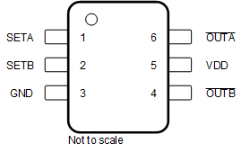
TMP392 DRL_SOT-563_pin_diagram_final.gif

Pin Functions

PIN I/O DESCRIPTION
NO. NAME
1 SETA Input Channel A temperature set point. Connect a standard E96, 1% resistance between SETA and GND.
2 SETB Input Channel B temperature and Hysteresis set point. Connect a standard E96, 1% resistance between SETB and GND.
3 GND Ground Device ground.
4 OUTB Logic Output Channel B logic open-drain active low output. If unused, the output can be left floating or connected to GND.
5 VDD Supply Power supply voltage (1.62 V – 5.5 V).
6 OUTA Logic Output Channel A logic open-drain active low output. If unused, the output can be left floating or connected to GND.