SBOS721A October   2014  – June 2022 TMP75B-Q1

PRODUCTION DATA  

  1. Features
  2. Applications
  3. Description
  4. Revision History
  5. Pin Configuration and Functions
  6. Specifications
    1. 6.1 Absolute Maximum Ratings
    2. 6.2 ESD Ratings
    3. 6.3 Recommended Operating Conditions
    4. 6.4 Thermal Information
    5. 6.5 Electrical Characteristics
    6. 6.6 Typical Characteristics
  7. Detailed Description
    1. 7.1 Overview
    2. 7.2 Functional Block Diagram
    3. 7.3 Feature Description
      1. 7.3.1 Digital Temperature Output
      2. 7.3.2 Temperature Limits and Alert
      3. 7.3.3 Serial Interface
        1. 7.3.3.1  Bus Overview
        2. 7.3.3.2  Serial Bus Address
        3. 7.3.3.3  Writing and Reading Operation
        4. 7.3.3.4  Target-Mode Operations
          1. 7.3.3.4.1 Target Receiver Mode:
          2. 7.3.3.4.2 Target Transmitter Mode:
        5. 7.3.3.5  SMBus Alert Function
        6. 7.3.3.6  General Call
        7. 7.3.3.7  High-Speed (Hs) Mode
        8. 7.3.3.8  Timeout Function
        9. 7.3.3.9  Two-Wire Timing
        10. 7.3.3.10 Two-Wire Timing Diagrams
    4. 7.4 Device Functional Modes
      1. 7.4.1 Continuous-Conversion Mode
      2. 7.4.2 Shutdown Mode
      3. 7.4.3 One-Shot Mode
    5. 7.5 Programming
    6. 7.6 Register Map
  8. Application and Implementation
    1. 8.1 Application Information
    2. 8.2 Typical Application
      1. 8.2.1 Design Requirements
      2. 8.2.2 Detailed Design Procedure
      3. 8.2.3 Application Curve
  9. Power-Supply Recommendations
  10. 10Layout
    1. 10.1 Layout Guidelines
    2. 10.2 Layout Example
  11. 11Device and Documentation Support
    1. 11.1 Documentation Support
      1. 11.1.1 Related Documentation
    2. 11.2 Trademarks
  12. 12Mechanical, Packaging, and Orderable Information

Package Options

Mechanical Data (Package|Pins)
Thermal pad, mechanical data (Package|Pins)
Orderable Information

Programming

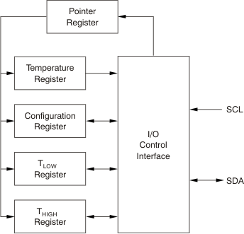
Figure 7-7 shows the internal register structure of the TMP75B-Q1. Use the 8-bit pointer register to address a given data register. The pointer register uses the two LSBs to identify which of the data registers respond to a read or write command. Figure 7-8 identifies the bits of the pointer register byte.
GUID-0D015CDC-A1D1-4CD2-86D5-4AD96739F71B-low.gif Figure 7-7 Internal Register Structure