SPRS439Q June 2007 – August 2022 TMS320F28232 , TMS320F28232-Q1 , TMS320F28234 , TMS320F28234-Q1 , TMS320F28235 , TMS320F28235-Q1 , TMS320F28332 , TMS320F28333 , TMS320F28334 , TMS320F28335 , TMS320F28335-Q1
PRODUCTION DATA
- 1 Features
- 2 Applications
- 3 Description
- 4 Revision History
- 5 Device Comparison
- 6 Terminal Configuration and Functions
-
7 Specifications
- 7.1 Absolute Maximum Ratings
- 7.2 ESD Ratings – Automotive
- 7.3 ESD Ratings – Commercial
- 7.4 Recommended Operating Conditions
- 7.5 Power Consumption Summary
- 7.6 Electrical Characteristics
- 7.7 Thermal Resistance Characteristics
- 7.8 Thermal Design Considerations
- 7.9
Timing and Switching Characteristics
- 7.9.1 Timing Parameter Symbology
- 7.9.2 Power Sequencing
- 7.9.3 Clock Requirements and Characteristics
- 7.9.4
Peripherals
- 7.9.4.1
General-Purpose Input/Output (GPIO)
- 7.9.4.1.1 GPIO - Output Timing
- 7.9.4.1.2 GPIO - Input Timing
- 7.9.4.1.3 Sampling Window Width for Input Signals
- 7.9.4.1.4
Low-Power Mode Wakeup Timing
- 7.9.4.1.4.1 IDLE Mode Timing Requirements
- 7.9.4.1.4.2 IDLE Mode Switching Characteristics
- 7.9.4.1.4.3 IDLE Mode Timing Diagram
- 7.9.4.1.4.4 STANDBY Mode Timing Requirements
- 7.9.4.1.4.5 STANDBY Mode Switching Characteristics
- 7.9.4.1.4.6 STANDBY Mode Timing Diagram
- 7.9.4.1.4.7 HALT Mode Timing Requirements
- 7.9.4.1.4.8 HALT Mode Switching Characteristics
- 7.9.4.1.4.9 HALT Mode Timing Diagram
- 7.9.4.2 Enhanced Control Peripherals
- 7.9.4.3 External Interrupt Timing
- 7.9.4.4 I2C Electrical Specification and Timing
- 7.9.4.5 Serial Peripheral Interface (SPI) Timing
- 7.9.4.6
Multichannel Buffered Serial Port (McBSP) Timing
- 7.9.4.6.1 McBSP Transmit and Receive Timing
- 7.9.4.6.2
McBSP as SPI Master or Slave Timing
- 7.9.4.6.2.1 McBSP as SPI Master or Slave Timing Requirements (CLKSTP = 10b, CLKXP = 0)
- 7.9.4.6.2.2 McBSP as SPI Master or Slave Switching Characteristics (CLKSTP = 10b, CLKXP = 0)
- 7.9.4.6.2.3 McBSP as SPI Master or Slave Timing Requirements (CLKSTP = 11b, CLKXP = 0)
- 7.9.4.6.2.4 McBSP as SPI Master or Slave Switching Characteristics (CLKSTP = 11b, CLKXP = 0)
- 7.9.4.6.2.5 McBSP as SPI Master or Slave Timing Requirements (CLKSTP = 10b, CLKXP = 1)
- 7.9.4.6.2.6 McBSP as SPI Master or Slave Switching Characteristics (CLKSTP = 10b, CLKXP = 1)
- 7.9.4.6.2.7 McBSP as SPI Master or Slave Timing Requirements (CLKSTP = 11b, CLKXP = 1)
- 7.9.4.6.2.8 McBSP as SPI Master or Slave Switching Characteristics (CLKSTP = 11b, CLKXP = 1)
- 7.9.4.1
General-Purpose Input/Output (GPIO)
- 7.9.5 JTAG Debug Probe Connection Without Signal Buffering for the MCU
- 7.9.6
External Interface (XINTF) Timing
- 7.9.6.1 USEREADY = 0
- 7.9.6.2 Synchronous Mode (USEREADY = 1, READYMODE = 0)
- 7.9.6.3 Asynchronous Mode (USEREADY = 1, READYMODE = 1)
- 7.9.6.4 XINTF Signal Alignment to XCLKOUT
- 7.9.6.5 External Interface Read Timing
- 7.9.6.6 External Interface Write Timing
- 7.9.6.7
External Interface Ready-on-Read Timing With One External Wait State
- 7.9.6.7.1 External Interface Read Switching Characteristics (Ready-on-Read, One Wait State)
- 7.9.6.7.2 External Interface Read Timing Requirements (Ready-on-Read, One Wait State)
- 7.9.6.7.3 Synchronous XREADY Timing Requirements (Ready-on-Read, One Wait State)
- 7.9.6.7.4 Asynchronous XREADY Timing Requirements (Ready-on-Read, One Wait State)
- 7.9.6.8 External Interface Ready-on-Write Timing With One External Wait State
- 7.9.6.9 XHOLD and XHOLDA Timing
- 7.9.7 Flash Timing
- 7.10 On-Chip Analog-to-Digital Converter
- 7.11 Migrating Between F2833x Devices and F2823x Devices
-
8 Detailed Description
- 8.1
Brief Descriptions
- 8.1.1 C28x CPU
- 8.1.2 Memory Bus (Harvard Bus Architecture)
- 8.1.3 Peripheral Bus
- 8.1.4 Real-Time JTAG and Analysis
- 8.1.5 External Interface (XINTF)
- 8.1.6 Flash
- 8.1.7 M0, M1 SARAMs
- 8.1.8 L0, L1, L2, L3, L4, L5, L6, L7 SARAMs
- 8.1.9 Boot ROM
- 8.1.10 Security
- 8.1.11 Peripheral Interrupt Expansion (PIE) Block
- 8.1.12 External Interrupts (XINT1–XINT7, XNMI)
- 8.1.13 Oscillator and PLL
- 8.1.14 Watchdog
- 8.1.15 Peripheral Clocking
- 8.1.16 Low-Power Modes
- 8.1.17 Peripheral Frames 0, 1, 2, 3 (PFn)
- 8.1.18 General-Purpose Input/Output (GPIO) Multiplexer
- 8.1.19 32-Bit CPU-Timers (0, 1, 2)
- 8.1.20 Control Peripherals
- 8.1.21 Serial Port Peripherals
- 8.2
Peripherals
- 8.2.1 DMA Overview
- 8.2.2 32-Bit CPU-Timer 0, CPU-Timer 1, CPU-Timer 2
- 8.2.3 Enhanced PWM Modules
- 8.2.4 High-Resolution PWM (HRPWM)
- 8.2.5 Enhanced CAP Modules
- 8.2.6 Enhanced QEP Modules
- 8.2.7 Analog-to-Digital Converter (ADC) Module
- 8.2.8 Multichannel Buffered Serial Port (McBSP) Module
- 8.2.9 Enhanced Controller Area Network (eCAN) Modules (eCAN-A and eCAN-B)
- 8.2.10 Serial Communications Interface (SCI) Modules (SCI-A, SCI-B, SCI-C)
- 8.2.11 Serial Peripheral Interface (SPI) Module (SPI-A)
- 8.2.12 Inter-Integrated Circuit (I2C)
- 8.2.13 GPIO MUX
- 8.2.14 External Interface (XINTF)
- 8.3 Memory Maps
- 8.4 Register Map
- 8.5 Interrupts
- 8.6 System Control
- 8.7 Low-Power Modes Block
- 8.1
Brief Descriptions
- 9 Applications, Implementation, and Layout
- 10Device and Documentation Support
- 11Mechanical, Packaging, and Orderable Information
Package Options
Refer to the PDF data sheet for device specific package drawings
Mechanical Data (Package|Pins)
- ZJZ|176
- ZAY|179
- PGF|176
- PTP|176
Thermal pad, mechanical data (Package|Pins)
- PTP|176
Orderable Information
8.5 Interrupts
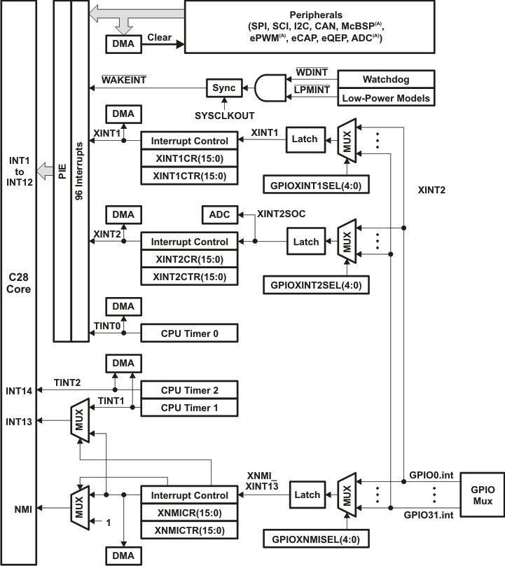
Figure 8-26 shows how the various interrupt sources are multiplexed.

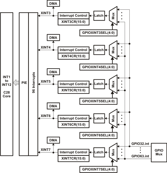
 Figure 8-27 External Interrupts
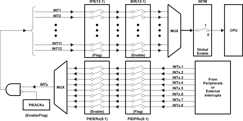
Eight PIE block interrupts are grouped into one CPU interrupt. In total, 12 CPU interrupt groups, with 8 interrupts per group equals 96 possible interrupts. On the 2833x/2823x devices, 58 of these are used by peripherals as shown in Table 8-32.
The TRAP #VectorNumber instruction transfers program control to the interrupt service routine corresponding to the vector specified. TRAP #0 tries to transfer program control to the address pointed to by the reset vector. The PIE vector table does not, however, include a reset vector. Therefore, TRAP #0 should not be used when the PIE is enabled. Doing so will result in undefined behavior.
When the PIE is enabled, TRAP #1 to TRAP #12 will transfer program control to the interrupt service routine corresponding to the first vector within the PIE group. For example: TRAP #1 fetches the vector from INT1.1, TRAP #2 fetches the vector from INT2.1, and so forth.
 Figure 8-28 Multiplexing of Interrupts Using the PIE Block
| CPU INTERRUPTS | PIE INTERRUPTS(1) | |||||||
|---|---|---|---|---|---|---|---|---|
| INTx.8 | INTx.7 | INTx.6 | INTx.5 | INTx.4 | INTx.3 | INTx.2 | INTx.1 | |
| INT1 | WAKEINT (LPM/WD) | TINT0 (TIMER 0) | ADCINT(2) (ADC) | XINT2 | XINT1 | Reserved | SEQ2INT (ADC) | SEQ1INT (ADC) |
| INT2 | Reserved | Reserved | EPWM6_TZINT (ePWM6) | EPWM5_TZINT (ePWM5) | EPWM4_TZINT (ePWM4) | EPWM3_TZINT (ePWM3) | EPWM2_TZINT (ePWM2) | EPWM1_TZINT (ePWM1) |
| INT3 | Reserved | Reserved | EPWM6_INT (ePWM6) | EPWM5_INT (ePWM5) | EPWM4_INT (ePWM4) | EPWM3_INT (ePWM3) | EPWM2_INT (ePWM2) | EPWM1_INT (ePWM1) |
| INT4 | Reserved | Reserved | ECAP6_INT (eCAP6) | ECAP5_INT (eCAP5) | ECAP4_INT (eCAP4) | ECAP3_INT (eCAP3) | ECAP2_INT (eCAP2) | ECAP1_INT (eCAP1) |
| INT5 | Reserved | Reserved | Reserved | Reserved | Reserved | Reserved | EQEP2_INT (eQEP2) | EQEP1_INT (eQEP1) |
| INT6 | Reserved | Reserved | MXINTA (McBSP-A) | MRINTA (McBSP-A) | MXINTB (McBSP-B) | MRINTB (McBSP-B) | SPITXINTA (SPI-A) | SPIRXINTA (SPI-A) |
| INT7 | Reserved | Reserved | DINTCH6 (DMA) | DINTCH5 (DMA) | DINTCH4 (DMA) | DINTCH3 (DMA) | DINTCH2 (DMA) | DINTCH1 (DMA) |
| INT8 | Reserved | Reserved | SCITXINTC (SCI-C) | SCIRXINTC (SCI-C) | Reserved | Reserved | I2CINT2A (I2C-A) | I2CINT1A (I2C-A) |
| INT9 | ECAN1_INTB (CAN-B) | ECAN0_INTB (CAN-B) | ECAN1_INTA (CAN-A) | ECAN0_INTA (CAN-A) | SCITXINTB (SCI-B) | SCIRXINTB (SCI-B) | SCITXINTA (SCI-A) | SCIRXINTA (SCI-A) |
| INT10 | Reserved | Reserved | Reserved | Reserved | Reserved | Reserved | Reserved | Reserved |
| INT11 | Reserved | Reserved | Reserved | Reserved | Reserved | Reserved | Reserved | Reserved |
| INT12 | LUF (FPU) | LVF (FPU) | Reserved | XINT7 | XINT6 | XINT5 | XINT4 | XINT3 |
1) No peripheral within the group is asserting interrupts.
2) No peripheral interrupts are assigned to the group (example PIE group 11).
| NAME | ADDRESS | SIZE (x16) | DESCRIPTION(1) |
|---|---|---|---|
| PIECTRL | 0x0CE0 | 1 | PIE, Control Register |
| PIEACK | 0x0CE1 | 1 | PIE, Acknowledge Register |
| PIEIER1 | 0x0CE2 | 1 | PIE, INT1 Group Enable Register |
| PIEIFR1 | 0x0CE3 | 1 | PIE, INT1 Group Flag Register |
| PIEIER2 | 0x0CE4 | 1 | PIE, INT2 Group Enable Register |
| PIEIFR2 | 0x0CE5 | 1 | PIE, INT2 Group Flag Register |
| PIEIER3 | 0x0CE6 | 1 | PIE, INT3 Group Enable Register |
| PIEIFR3 | 0x0CE7 | 1 | PIE, INT3 Group Flag Register |
| PIEIER4 | 0x0CE8 | 1 | PIE, INT4 Group Enable Register |
| PIEIFR4 | 0x0CE9 | 1 | PIE, INT4 Group Flag Register |
| PIEIER5 | 0x0CEA | 1 | PIE, INT5 Group Enable Register |
| PIEIFR5 | 0x0CEB | 1 | PIE, INT5 Group Flag Register |
| PIEIER6 | 0x0CEC | 1 | PIE, INT6 Group Enable Register |
| PIEIFR6 | 0x0CED | 1 | PIE, INT6 Group Flag Register |
| PIEIER7 | 0x0CEE | 1 | PIE, INT7 Group Enable Register |
| PIEIFR7 | 0x0CEF | 1 | PIE, INT7 Group Flag Register |
| PIEIER8 | 0x0CF0 | 1 | PIE, INT8 Group Enable Register |
| PIEIFR8 | 0x0CF1 | 1 | PIE, INT8 Group Flag Register |
| PIEIER9 | 0x0CF2 | 1 | PIE, INT9 Group Enable Register |
| PIEIFR9 | 0x0CF3 | 1 | PIE, INT9 Group Flag Register |
| PIEIER10 | 0x0CF4 | 1 | PIE, INT10 Group Enable Register |
| PIEIFR10 | 0x0CF5 | 1 | PIE, INT10 Group Flag Register |
| PIEIER11 | 0x0CF6 | 1 | PIE, INT11 Group Enable Register |
| PIEIFR11 | 0x0CF7 | 1 | PIE, INT11 Group Flag Register |
| PIEIER12 | 0x0CF8 | 1 | PIE, INT12 Group Enable Register |
| PIEIFR12 | 0x0CF9 | 1 | PIE, INT12 Group Flag Register |
| Reserved | 0x0CFA – 0x0CFF | 6 | Reserved |