SCDS406A December 2018 – February 2024 TMUX1109
PRODUCTION DATA
- 1
- 1 Features
- 2 Applications
- 3 Description
- 4 Pin Configuration and Functions
-
5 Specifications
- 5.1 Absolute Maximum Ratings
- 5.2 ESD Ratings
- 5.3 Recommended Operating Conditions
- 5.4 Thermal Information
- 5.5 Electrical Characteristics (VDD = 5V ±10 %)
- 5.6 Electrical Characteristics (VDD = 3.3V ±10 %)
- 5.7 Electrical Characteristics (VDD = 2.5V ±10 %), (VSS = –2.5V ±10 %)
- 5.8 Electrical Characteristics (VDD = 1.8V ±10 %)
- 5.9 Electrical Characteristics (VDD = 1.2V ±10 %)
- Typical Characteristics
- 6 Detailed Description
- 7 Application and Implementation
- 8 Device and Documentation Support
- 9 Revision History
- 10Mechanical, Packaging, and Orderable Information
Package Options
Refer to the PDF data sheet for device specific package drawings
Mechanical Data (Package|Pins)
- PW|16
- RSV|16
Thermal pad, mechanical data (Package|Pins)
Orderable Information
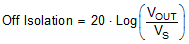
6.1.8 Off Isolation
Off isolation is defined as the ratio of the signal at the drain pin (D) of the device when a signal is applied to the source pin (Sx) of an off-channel. Figure 6-8 shows the setup used to measure and the equation used to compute off isolation.
 Figure 6-8 Off Isolation Measurement Setup
Equation 1.