SCDS389C August 2018 – December 2018 TMUX1208 , TMUX1209
PRODUCTION DATA.
- 1 Features
- 2 Applications
- 3 Description
- 4 Revision History
- 5 Device Comparison Table
- 6 Pin Configuration and Functions
-
7 Specifications
- 7.1 Absolute Maximum Ratings
- 7.2 ESD Ratings
- 7.3 Recommended Operating Conditions
- 7.4 Thermal Information
- 7.5 Electrical Characteristics (VDD = 5 V ±10 %)
- 7.6 Electrical Characteristics (VDD = 3.3 V ±10 %)
- 7.7 Electrical Characteristics (VDD = 1.8 V ±10 %)
- 7.8 Electrical Characteristics (VDD = 1.2 V ±10 %)
- 7.9 Typical Characteristics
- 8 Detailed Description
- 9 Application and Implementation
- 10Power Supply Recommendations
- 11Layout
- 12Device and Documentation Support
- 13Mechanical, Packaging, and Orderable Information
Package Options
Mechanical Data (Package|Pins)
Thermal pad, mechanical data (Package|Pins)
Orderable Information
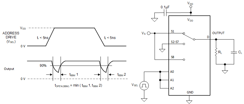
8.1.5 Break-Before-Make
Break-before-make delay is a safety feature that prevents two inputs from connecting when the device is switching. The output first breaks from the on-state switch before making the connection with the next on-state switch. The time delay between the break and the make is known as break-before-make delay. Figure 11 shows the setup used to measure break-before-make delay, denoted by the symbol tOPEN(BBM).
 Figure 11. Break-Before-Make Delay Measurement Setup