SCDS447 July   2021 TMUX1248

PRODUCTION DATA  

  1. Features
  2. Applications
  3. Description
  4. Revision History
  5. Pin Configuration and Functions
  6. Specifications
    1. 6.1 Absolute Maximum Ratings
    2. 6.2 ESD Ratings
    3. 6.3 Recommended Operating Conditions
    4. 6.4 Thermal Information
    5. 6.5 Electrical Characteristics (VDD = 5 V ±10 %), GND = 0 V unless otherwise specified.
    6. 6.6 Electrical Characteristics (VDD = 3.3 V ±10 %), GND = 0 V unless otherwise specified.
    7. 6.7 Electrical Characteristics (VDD = 1.8 V ±10 %), GND = 0 V unless otherwise specified.
    8. 6.8 Electrical Characteristics (VDD = 1.2 V ±10 %), GND = 0 V unless otherwise specified.
    9. 6.9 Typical Characteristics
  7. Parameter Measurement Information
    1. 7.1 On-Resistance
    2. 7.2 Off-Leakage Current
    3. 7.3 On-Leakage Current
    4. 7.4 Transition Time
    5. 7.5 Break-Before-Make
    6. 7.6 Charge Injection
    7. 7.7 Off Isolation
    8. 7.8 Crosstalk
    9. 7.9 Bandwidth
  8. Detailed Description
    1. 8.1 Overview
    2. 8.2 Functional Block Diagram
    3. 8.3 Feature Description
      1. 8.3.1 Bidirectional Operation
      2. 8.3.2 Rail to Rail Operation
      3. 8.3.3 1.8 V Logic Compatible Inputs
      4. 8.3.4 Fail-Safe Logic
    4. 8.4 Device Functional Modes
    5. 8.5 Truth Tables
  9. Power Supply Recommendations
  10. 10Layout
    1. 10.1 Layout Guidelines
      1. 10.1.1 Layout Information
    2. 10.2 Layout Example
  11. 11Device and Documentation Support
    1. 11.1 Documentation Support
      1. 11.1.1 Related Documentation
    2. 11.2 Receiving Notification of Documentation Updates
    3. 11.3 Support Resources
    4. 11.4 Trademarks
    5. 11.5 Electrostatic Discharge Caution
    6. 11.6 Glossary
  12. 12Mechanical, Packaging, and Orderable Information

Package Options

Mechanical Data (Package|Pins)
Thermal pad, mechanical data (Package|Pins)
Orderable Information

Typical Characteristics

At TA = 25°C, VDD = 5 V (unless otherwise noted).
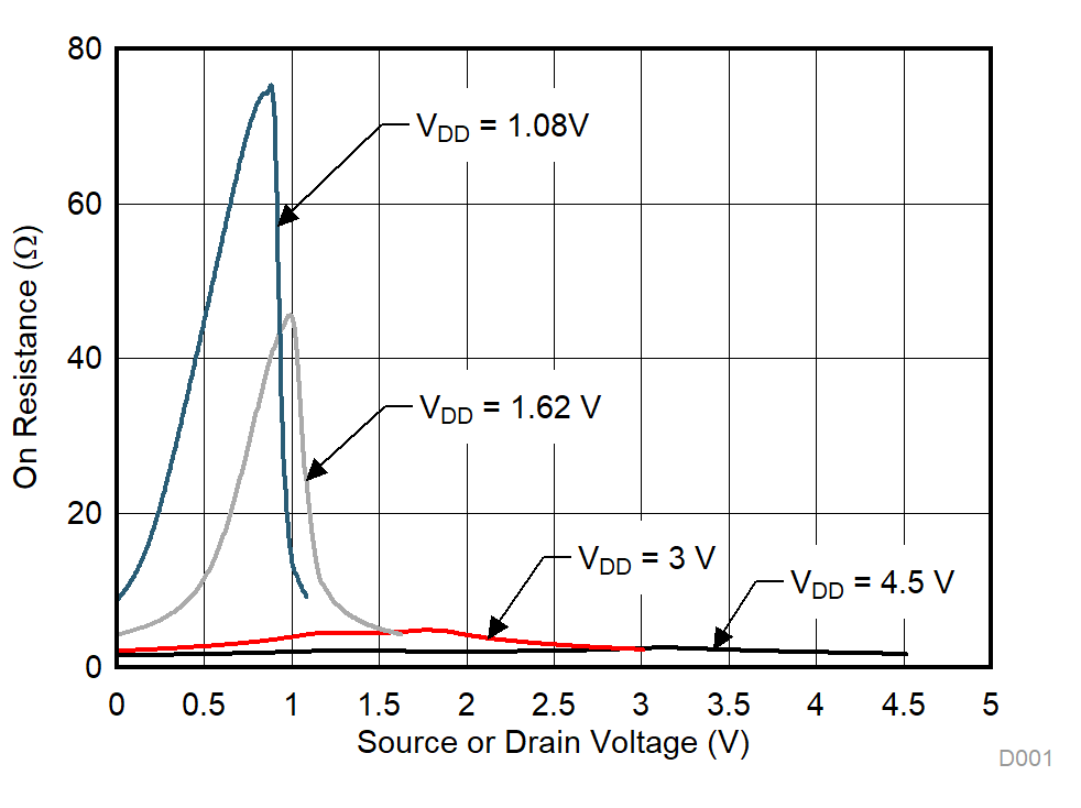
GUID-A1985A86-F9A1-4DD2-A3B6-924980030F4B-low.gif
TA = 25°C
Figure 6-1 On-Resistance vs Source or Drain Voltage
GUID-4CFE950E-E62B-4689-A282-D6C7004786EE-low.gif
TA = 25°C
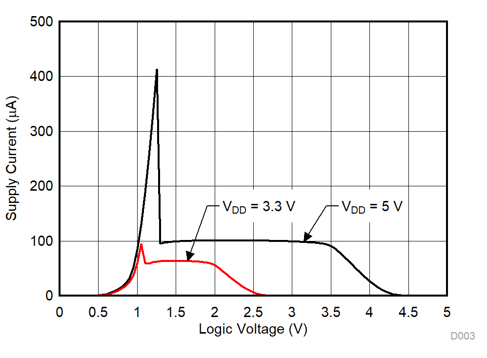
Figure 6-3 Supply Current vs Logic Voltage
GUID-41D8A409-4977-4D6D-B2A3-558618DB932C-low.gif
TA = 25°C
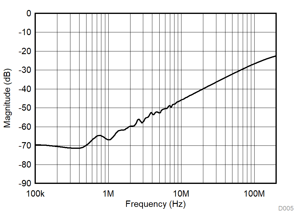
Figure 6-5 Crosstalk and Off-Isolation vs Frequency
GUID-ED91A1CD-7D7C-41E4-90DC-C4BC5433383C-low.gif
VDD = 3 V
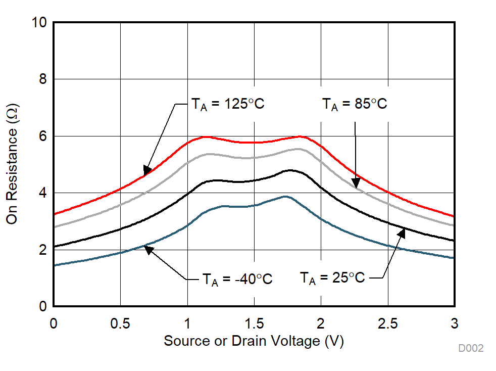
Figure 6-2 On-Resistance vs Source or Drain Voltage
GUID-9EC8D22B-AAFE-4746-8C1B-908F43423F2E-low.gif
TA = 25°C
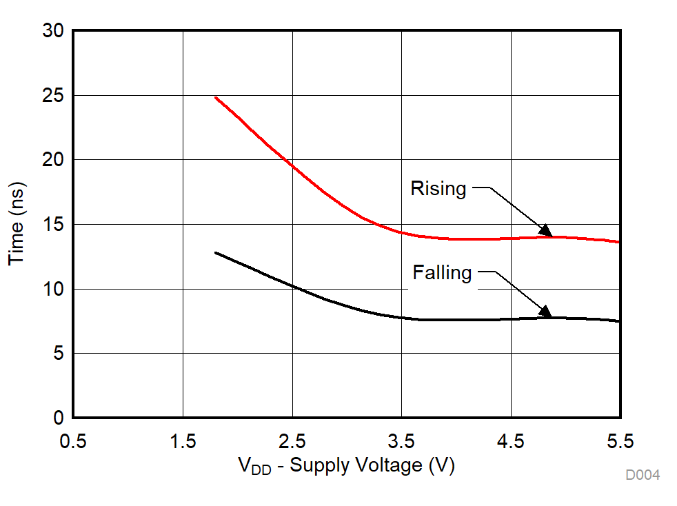
Figure 6-4 Ttransition vs Supply Voltage
GUID-90CA4F34-3CBB-4E7B-933A-E6A8FBE4C8A0-low.gif
TA = 25°C
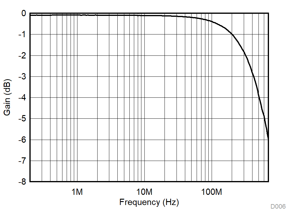
Figure 6-6 Frequency Response