SCDS379 February 2018 TMUX154E
PRODUCTION DATA.
- 1 Features
- 2 Applications
- 3 Description
- 4 Revision History
- 5 Pin Configuration and Functions
- 6 Specifications
- 7 Parameter Measurement Information
- 8 Detailed Description
- 9 Application and Implementation
- 10Power Supply Recommendations
- 11Layout
- 12Device and Documentation Support
- 13Mechanical, Packaging, and Orderable Information
Package Options
Mechanical Data (Package|Pins)
Thermal pad, mechanical data (Package|Pins)
Orderable Information
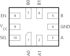
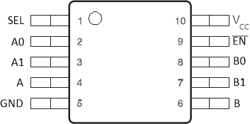
5 Pin Configuration and Functions
RSW Package
10-PIN UQFN
Top View

DGS Package
10-PIN VSSOP
Top View

Pin Functions
| PIN | I/O | DESCRIPTION | ||
|---|---|---|---|---|
| NAME | UQFN | VSSOP | ||
| A0 | 1 | 2 | I/O | signal path port 0 |
| B0 | 7 | 8 | I/O | |
| A | 3 | 4 | I/O | Common signal path |
| B | 5 | 6 | I/O | |
| A1 | 2 | 3 | I/O | signal path port 1 |
| B1 | 6 | 7 | I/O | |
| EN | 8 | 9 | I | EN = 0 Enable EN = 1 Disable |
| SEL | 10 | 1 | I | Select input: SEL = 0 A,B to A0,B0 SEL = 1 A,B to A1,B1 |
| GND | 4 | 5 | — | Ground |
| VCC | 9 | 10 | — | Voltage supply |