SCDS376A February 2018 – September 2018 TMUX6104
PRODUCTION DATA.
- 1 Features
- 2 Applications
- 3 Description
- 4 Revision History
- 5 Pin Configuration and Functions
-
6 Specifications
- 6.1 Absolute Maximum Ratings
- 6.2 ESD Ratings
- 6.3 Thermal Information
- 6.4 Recommended Operating Conditions
- 6.5 Electrical Characteristics (Dual Supplies: ±15 V)
- 6.6 Switching Characteristics (Dual Supplies: ±15 V)
- 6.7 Electrical Characteristics (Single Supply: 12 V)
- 6.8 Switching Characteristics (Single Supply: 12 V)
- 6.9 Typical Characteristics
- 7 Parameter Measurement Information
-
8 Detailed Description
- 8.1
Overview
- 8.1.1 On-Resistance
- 8.1.2 Off-Leakage Current
- 8.1.3 On-Leakage Current
- 8.1.4 Transition Time
- 8.1.5 Break-Before-Make Delay
- 8.1.6 Turn-On and Turn-Off Time
- 8.1.7 Charge Injection
- 8.1.8 Off Isolation
- 8.1.9 Channel-to-Channel Crosstalk
- 8.1.10 Bandwidth
- 8.1.11 THD + Noise
- 8.1.12 AC Power Supply Rejection Ratio (AC PSRR)
- 8.2 Functional Block Diagram
- 8.3 Feature Description
- 8.4 Device Functional Modes
- 8.1
Overview
- 9 Application and Implementation
- 10Power Supply Recommendations
- 11Layout
- 12Device and Documentation Support
- 13Mechanical, Packaging, and Orderable Information
Package Options
Mechanical Data (Package|Pins)
- PW|14
Thermal pad, mechanical data (Package|Pins)
Orderable Information
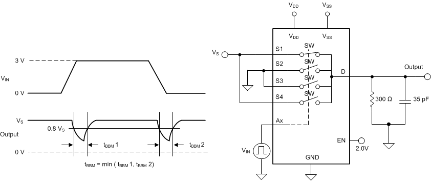
8.1.5 Break-Before-Make Delay
Break-before-make delay is a safety feature that prevents two inputs from connecting when the TMUX6104 is switching. The TMUX6104 output first breaks from the on-state switch before making the connection with the next on-state switch. The time delay between the break and the make is known as break-before-make delay. Figure 21 shows the setup used to measure break-before-make delay, denoted by the symbol tBBM.
 Figure 21. Break-Before-Make Delay Measurement Setup