SLOS275E January   2000  – November 2016 TPA0211

PRODUCTION DATA.  

  1. Features
  2. Applications
  3. Description
  4. Revision History
  5. Device Comparison Table
  6. Pin Configuration and Functions
  7. Specifications
    1. 7.1 Absolute Maximum Ratings
    2. 7.2 ESD Ratings
    3. 7.3 Recommended Operating Conditions
    4. 7.4 Thermal Information
    5. 7.5 Electrical Characteristics - 3 V
    6. 7.6 Electrical Characteristics - 5 V
    7. 7.7 Dissipation Ratings
    8. 7.8 Typical Characteristics
  8. Parameter Measurement Information
    1. 8.1 Set-Up for Graphs
  9. Detailed Description
    1. 9.1 Overview
    2. 9.2 Functional Block Diagram
    3. 9.3 Feature Description
      1. 9.3.1 Bridged-Tied Load Versus Single-Ended Mode
      2. 9.3.2 Single-Ended Operation
      3. 9.3.3 BTL Amplifier Efficiency
      4. 9.3.4 Gain Setting Via Input Resistance
      5. 9.3.5 Crest Factor
    4. 9.4 Device Functional Modes
      1. 9.4.1 Shutdown Mode
      2. 9.4.2 SE/BTL (Stereo/Mono) Operation
  10. 10Application and Implementation
    1. 10.1 Application Information
    2. 10.2 Typical Application
      1. 10.2.1 Design Requirements
      2. 10.2.2 Detailed Design Procedure
        1. 10.2.2.1 Surface Mount Capacitor
        2. 10.2.2.2 Input Capacitor, Ci
        3. 10.2.2.3 Power Supply Decoupling, C(S)
        4. 10.2.2.4 Midrail Bypass Capacitor, C(BYP)
        5. 10.2.2.5 Output Coupling Capacitor, C(C)
      3. 10.2.3 Application Curves
  11. 11Power Supply Recommendations
    1. 11.1 Power Supply Decoupling Capacitors
  12. 12Layout
    1. 12.1 Layout Guidelines
      1. 12.1.1 Component Placement
    2. 12.2 Layout Example
    3. 12.3 Thermal Considerations
  13. 13Device and Documentation Support
    1. 13.1 Documentation Support
      1. 13.1.1 Related Documentation
    2. 13.2 Receiving Notification of Documentation Updates
    3. 13.3 Community Resources
    4. 13.4 Trademarks
    5. 13.5 Electrostatic Discharge Caution
    6. 13.6 Glossary
  14. 14Mechanical, Packaging, and Orderable Information

Package Options

Refer to the PDF data sheet for device specific package drawings

Mechanical Data (Package|Pins)
  • DGN|8
Thermal pad, mechanical data (Package|Pins)
Orderable Information

Parameter Measurement Information

Set-Up for Graphs

All parameters are measured according to the conditions described in Specifications. Figure 22 shows the setup used for the typical characteristics of the test device.
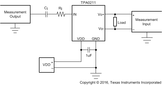
TPA0211 Test_Set_Up_for_Graphs.gif
All other measurements were taken with 1-µF CI (unless otherwise noted).
A 33-µH inductor was placed in series with the load resistor to emulate a small speaker for efficiency measurements.
Figure 22. Test Set-Up for Graphs