SLOS942 April 2018 TPA3126D2
PRODUCTION DATA.
- 1 Features
- 2 Applications
- 3 Description
- 4 Revision History
- 5 Device Comparison Table
- 6 Pin Configuration and Functions
- 7 Specifications
-
8 Detailed Description
- 8.1 Overview
- 8.2 Functional Block Diagram
- 8.3
Feature Description
- 8.3.1 Gain Setting and Master and Slave
- 8.3.2 Input Impedance
- 8.3.3 Startup and Shutdown Operation
- 8.3.4 PLIMIT Operation
- 8.3.5 GVDD Supply
- 8.3.6 BSPx and BSNx Capacitors
- 8.3.7 Differential Inputs
- 8.3.8 Device Protection System
- 8.3.9 DC Detect Protection
- 8.3.10 Short-Circuit Protection and Automatic Recovery Feature
- 8.3.11 Thermal Protection
- 8.3.12 Device Modulation Scheme
- 8.3.13 Efficiency: LC Filter Required with the Traditional Class-D Modulation Scheme
- 8.3.14 Ferrite Bead Filter Considerations
- 8.3.15 When to Use an Output Filter for EMI Suppression
- 8.3.16 AM Avoidance EMI Reduction
- 8.4 Device Functional Modes
- 9 Application and Implementation
- 10Power Supply Recommendations
- 11Layout
- 12Device and Documentation Support
- 13Mechanical, Packaging, and Orderable Information
Package Options
Mechanical Data (Package|Pins)
- DAD|32
Thermal pad, mechanical data (Package|Pins)
- DAD|32
Orderable Information
8.3.4 PLIMIT Operation
The TPA3126D2 has a built-in voltage limiter that can be used to limit the output voltage level below the supply rail. The amplifier operates as if it was powered by a lower supply voltage, and thereby, limits the output power. Add a resistor divider from GVDD to ground to set the voltage at the PLIMIT pin. An external reference may also be used if tighter tolerance is required. Add a 1-µF capacitor from pin PLIMIT to ground to ensure stability.
 Figure 27. Power Limit Example
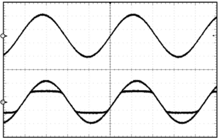
The PLIMIT circuit sets a limit on the output peak-to-peak voltage. This is done by limiting the duty cycle to a fixed maximum value. The limit can be considered as a "virtual" voltage rail which is lower than the supply connected to PVCC. The "virtual" rail is approximately four times the voltage at the PLIMIT pin. The output voltage can be used to calculate the maximum output power for a given maximum input voltage and speaker impedance.

where
- POUT (10%THD) = 1.25 × POUT (unclipped)
- RL is the load resistance.
- RS is the total series resistance including RDS(on), and output filter resistance.
- VP is the peak amplitude, which is limited by the "virtual" voltage rail.
Table 3. Power Limit Example
| PVCC (V) | PLIMIT VOLTAGE (V)(1) | R to GND | R to GVDD | OUTPUT VOLTAGE (Vrms) |
|---|---|---|---|---|
| 24 V | GVDD | Open | Short | 17.9 |
| 24 V | 3.3 | 45 kΩ | 51 kΩ | 12.67 |
| 24 V | 2.25 | 24 kΩ | 51 kΩ | 9 |
| 12 V | GVDD | Open | Short | 10.33 |
| 12 V | 2.25 | 24 kΩ | 51 kΩ | 9 |
| 12 V | 1.5 | 18 kΩ | 68 kΩ | 6.3 |