SLASEN3B January   2018  – August 2018 TPA3220

PRODUCTION DATA.  

  1. Features
  2. Applications
  3. Description
    1.     Simplified Schematic
  4. Revision History
  5. Device Comparison Table
  6. Pin Configuration and Functions
    1.     Pin Functions
  7. Specifications
    1. 7.1 Absolute Maximum Ratings
    2. 7.2 ESD Ratings
    3. 7.3 Recommended Operating Conditions
    4. 7.4 Thermal Information
    5. 7.5 Electrical Characteristics
    6. 7.6 Audio Characteristics (BTL)
    7. 7.7 Audio Characteristics (PBTL)
    8. 7.8 Typical Characteristics, BTL Configuration, AD-mode
    9. 7.9 Typical Characteristics, PBTL Configuration, AD-mode
  8. Parameter Measurement Information
  9. Detailed Description
    1. 9.1 Overview
    2. 9.2 Functional Block Diagrams
    3. 9.3 Feature Description
      1. 9.3.1 Internal LDO
        1. 9.3.1.1 Input Configuration, Gain Setting And Master / Slave Operation
      2. 9.3.2 Gain Setting And Master / Slave Operation
      3. 9.3.3 AD-Mode and HEAD-Mode PWM Modulation
      4. 9.3.4 Oscillator
      5. 9.3.5 Input Impedance
      6. 9.3.6 Error Reporting
    4. 9.4 Device Functional Modes
      1. 9.4.1 Powering Up
        1. 9.4.1.1 Startup Ramp Time
      2. 9.4.2 Powering Down
        1. 9.4.2.1 Power Down Ramp Time
      3. 9.4.3 Device Reset
      4. 9.4.4 Device Soft Mute
      5. 9.4.5 Device Protection System
        1. 9.4.5.1 Overload and Short Circuit Current Protection
        2. 9.4.5.2 Signal Clipping and Pulse Injector
        3. 9.4.5.3 DC Speaker Protection
        4. 9.4.5.4 Pin-to-Pin Short Circuit Protection (PPSC)
        5. 9.4.5.5 Overtemperature Protection OTW and OTE
        6. 9.4.5.6 Undervoltage Protection (UVP) and Power-on Reset (POR)
        7. 9.4.5.7 Fault Handling
  10. 10Application and Implementation
    1. 10.1 Application Information
    2. 10.2 Typical Applications
      1. 10.2.1 Stereo BTL Application
        1. 10.2.1.1 Design Requirements
        2. 10.2.1.2 Detailed Design Procedures
          1. 10.2.1.2.1 Decoupling Capacitor Recommendations
          2. 10.2.1.2.2 PVDD Capacitor Recommendation
          3. 10.2.1.2.3 BST capacitors
          4. 10.2.1.2.4 PCB Material Recommendation
      2. 10.2.2 Typical Application, Differential (2N), AD-Mode PBTL (Outputs Paralleled before LC filter)
        1. 10.2.2.1 Design Requirements
      3. 10.2.3 Typical Application, Differential (2N), AD-Mode PBTL (Outputs Paralleled after LC filter)
        1. 10.2.3.1 Design Requirements
  11. 11Power Supply Recommendations
    1. 11.1 Power Supplies
      1. 11.1.1 VDD Supply
      2. 11.1.2 AVDD and GVDD Supplies
      3. 11.1.3 PVDD Supply
      4. 11.1.4 BST Supply
  12. 12Layout
    1. 12.1 Layout Guidelines
    2. 12.2 Layout Examples
      1. 12.2.1 BTL Application Printed Circuit Board Layout Example
      2. 12.2.2 PBTL (Outputs Paralleled before LC filter) Application Printed Circuit Board Layout Example
      3. 12.2.3 PBTL (Outputs Paralleled after LC filter) Application Printed Circuit Board Layout Example
  13. 13Device and Documentation Support
    1. 13.1 Documentation Support
    2. 13.2 Receiving Notification of Documentation Updates
    3. 13.3 Community Resources
    4. 13.4 Trademarks
    5. 13.5 Electrostatic Discharge Caution
    6. 13.6 Glossary
  14. 14Mechanical, Packaging, and Orderable Information

Package Options

Refer to the PDF data sheet for device specific package drawings

Mechanical Data (Package|Pins)
  • DDW|44
Thermal pad, mechanical data (Package|Pins)
Orderable Information

Typical Characteristics, PBTL Configuration, AD-mode

All Measurements taken at audio frequency = 1 kHz, PVDD_X = 30V, VDD = 5 V, GVDD = 5 V, RL = 2Ω, fS = 480 kHz, TA = 25°C, Output Filter: LDEM = 10 μH, CDEM = 1 µF, Pre-Filter PBTL, AD modulation, AES17 + AUX-0025 measurement filters, unless otherwise noted.
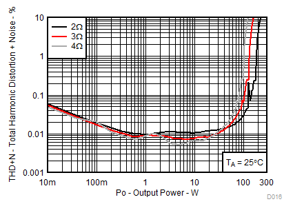
TPA3220 D016_SLASEN3.gif
RL = 2Ω, 3Ω, 4Ω
Figure 17. Total Harmonic Distortion+Noise vs Output Power
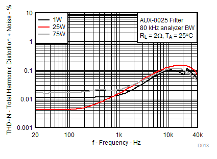
TPA3220 D018_SLASEN3.gif
RL = 2Ω P = 1W, 25W, 75W
AUX-0025 filter, 80 kHz analyzer BW
Figure 19. Total Harmonic Distortion+Noise vs Frequency, 80kHz Bandwidth
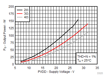
TPA3220 D020_SLASEN3.gif
RL = 2Ω, 3Ω, 4Ω THD+N = 1%
Figure 21. Output Power vs Supply Voltage
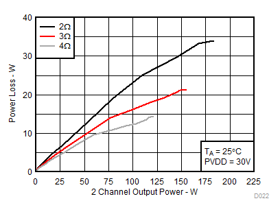
TPA3220 D022_SLASEN3.gif
RL = 2Ω, 3Ω, 4Ω
Figure 23. System Power Loss vs Output Power, AD-Mode
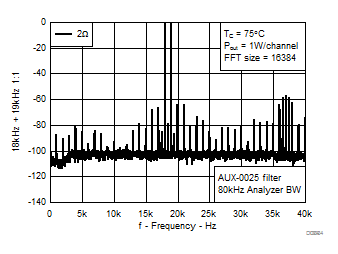
TPA3220 D024_SLASEE9.gif
Figure 25. CCIF Intermodulation vs Frequency, AD-mode
TPA3220 D017_SLASEN3.gif
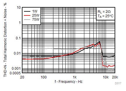
RL = 2Ω P = 1W, 25W, 75W
Figure 18. Total Harmonic Distortion+Noise vs Frequency
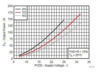
TPA3220 D019_SLASEN3.gif
RL = 2Ω, 3Ω, 4Ω THD+N = 10%
Figure 20. Output Power vs Supply Voltage
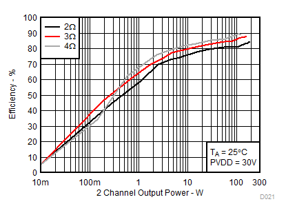
TPA3220 D021_SLASEN3.gif
RL = 2Ω, 4Ω, 8Ω THD+N = 10%
Figure 22. System Efficiency vs Output Power, AD-Mode
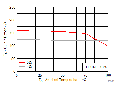
TPA3220 D023_SLASEN3.gif
Figure 24. Output Power vs Ambient Temperature
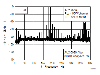
TPA3220 D025_SLASEE9.gif
Figure 26. CCIF Intermodulation vs Frequency, AD-mode