SLOS821B June 2013 – September 2014 TPA6133A2
PRODUCTION DATA.
- 1 Features
- 2 Applications
- 3 Description
- 4 Simplified Application Diagram
- 5 Revision History
- 6 Pin Configuration and Functions
- 7 Specification
- 8 Detailed Description
- 9 Application and Implementation
- 10Power Supply Recommendations
- 11Layout
- 12Device and Documentation Support
- 13Mechanical, Packaging, and Orderable Information
Package Options
Mechanical Data (Package|Pins)
- RTJ|20
Thermal pad, mechanical data (Package|Pins)
- RTJ|20
Orderable Information
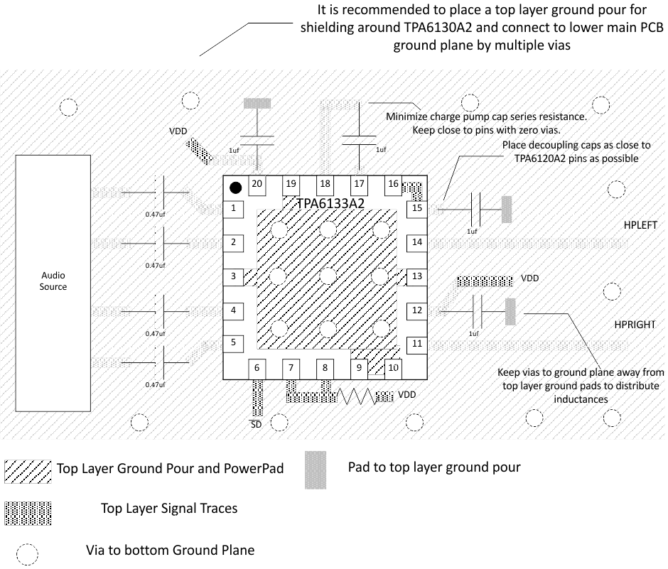
11 Layout
11.1 Layout Guidelimes
11.1.1 Exposed Pad On TPA6133A2RTJ Package
- Solder the exposed metal pad on the TPA6133A2RTJ QFN package to the a pad on the PCB. The pad on the PCB may be grounded or may be allowed to float (not be connected to ground or power).
- If the pad is grounded, it must be connected to the same ground as the GND pins (3, 9, 10, 13, and 19). See the layout and mechanical drawings at the end of the datasheet for proper sizing.
- Soldering the thermal pad improves mechanical reliability, improves grounding of the device, and enhances thermal conductivity of the package.
11.1.2 GND Connections
- The GND pin for charge pump should be decoupled to the charge pump VDD pin, and the GND pin adjacent to the Analog VDD pin should be separately decoupled to each other.