SLVS640F October 2007 – February 2015 TPD12S520
PRODUCTION DATA.
- 1 Features
- 2 Applications
- 3 Description
- 4 Revision History
- 5 Pin Configuration and Functions
- 6 Specifications
-
7 Detailed Description
- 7.1 Overview
- 7.2 Functional Block Diagram
- 7.3
Feature Description
- 7.3.1 ±8-kV Contact ESD Protection on External Lines
- 7.3.2 Single-Chip ESD Solution for HDMI Driver
- 7.3.3 Supports All HDMI 1.3 and HDMI 1.4b Data Rates
- 7.3.4 38-Pin TSSOP Provides Seamless Layout Option With HDMI Connector
- 7.3.5 24-Pin WQFNPackage for Space Constrained Applications
- 7.3.6 Integrated Level Shifting for the Control Lines
- 7.3.7 Backdrive Protection
- 7.3.8 Lead-Free Package
- 7.4 Device Functional Modes
- 8 Application and Implementation
- 9 Power Supply Recommendations
- 10Layout
- 11Device and Documentation Support
- 12Mechanical, Packaging, and Orderable Information
Package Options
Mechanical Data (Package|Pins)
Thermal pad, mechanical data (Package|Pins)
Orderable Information
10 Layout
10.1 Layout Guidelines
- The optimum placement is as close to the connector as possible.
- EMI during an ESD event can couple from the trace being struck to other nearby unprotected traces, resulting in early system failures.
- The PCB designer needs to minimize the possibility of EMI coupling by keeping any unprotected traces away from the protected traces which are between the TVS and the connector.
- Route the protected traces as straight as possible.
- Eliminate any sharp corners on the protected traces between the TVS and the connector by using rounded corners with the largest radii possible.
- Electric fields tend to build up on corners, increasing EMI coupling.
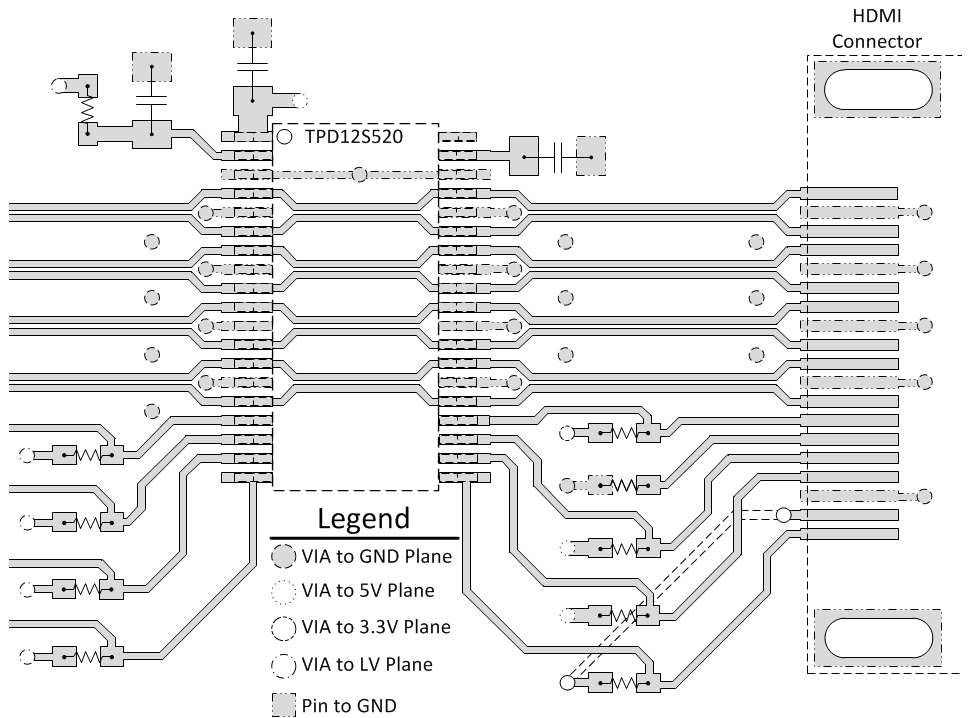
10.2 Layout Example
 Figure 10. TPD12S520DBT Layout Example
Use external and internal ground planes and stitch them together with VIAs as close to the GND pins of TPD12S520 as possible. This allows for a low impedance path to ground so that the device can properly dissipate an ESD event.