SLVSC77D August 2013 – April 2016 TPD2E1B06
PRODUCTION DATA.
- 1 Features
- 2 Applications
- 3 Description
- 4 Revision History
- 5 Pin Configuration and Functions
- 6 Specifications
- 7 Detailed Description
- 8 Application and Implementation
- 9 Power Supply Recommendations
- 10Layout
- 11Device and Documentation Support
- 12Mechanical, Packaging, and Orderable Information
Package Options
Mechanical Data (Package|Pins)
- DRL|6
Thermal pad, mechanical data (Package|Pins)
Orderable Information
6 Specifications
6.1 Absolute Maximum Ratings
over operating free-air temperature range (unless otherwise noted)(1)| MIN | MAX | UNIT | ||
|---|---|---|---|---|
| Operating temperature | –40 | 125 | °C | |
| IPP | Peak pulse current (tp = 8/20 μs)(2) | 2.5 | A | |
| PPP | Peak pulse power (tp = 8/20 μs)(2) | 35 | W | |
| Tstg | Storage temperature | –65 | 155 | °C |
(1) Stresses beyond those listed under Absolute Maximum Ratings may cause permanent damage to the device. These are stress ratings only, which do not imply functional operation of the device at these or any other conditions beyond those indicated under Recommended Operating Conditions. Exposure to absolute-maximum-rated conditions for extended periods may affect device reliability.
6.2 ESD Ratings
| VALUE | UNIT | |||
|---|---|---|---|---|
| V(ESD) | Electrostatic discharge | IEC 61000-4-2 contact discharge(2) | ±10000 | V |
| IEC 61000-4-2 air-gap discharge(2) | ±15000 | |||
6.3 Recommended Operating Conditions
over operating free-air temperature range (unless otherwise noted)| MIN | MAX | UNIT | ||
|---|---|---|---|---|
| VIO | Pin IOA1 to IOA2; Pin IOB1 to IOB2 | –5.5 | 5.5 | V |
| TA | Operating free-air temperature | –40 | 125 | °C |
6.4 Thermal Information
over operating free-air temperature range (unless otherwise noted)| THERMAL METRIC(1) | TPD2E1B06 | UNIT | |
|---|---|---|---|
| DRL (SOT) | |||
| 6 PINS | |||
| RθJA | Junction-to-ambient thermal resistance | 349.7 | ºC/W |
| RθJC(top) | Junction-to-case (top) thermal resistance | 120.5 | ºC/W |
| RθθJB | Junction-to-board thermal resistance | 171.4 | ºC/W |
| ψJT | Junction-to-top characterization parameter | 10.8 | ºC/W |
| ψJB | Junction-to-board characterization parameter | 169.4 | ºC/W |
(1) For more information about traditional and new thermal metrics, the Semiconductor and IC Package Thermal Metrics application report, SPRA953.
6.5 Electrical Characteristics
over operating free-air temperature range. (unless otherwise noted)| PARAMETER | TEST CONDITIONS | MIN | TYP | MAX | UNIT | |
|---|---|---|---|---|---|---|
| VRWM | Reverse standoff voltage | 5.5 | V | |||
| VCLAMP | Clamp voltage with ESD strike | IPP = 1 A, TLP, I/O to GND(1)(2) | 11 | V | ||
| IPP = 5 A, TLP, I/O to GND(1)(2) | 15 | |||||
| VCLAMP | Clamp voltage with ESD strike | IPP = 1 A, TLP, GND to I/O (1)(2) | 11 | V | ||
| IPP = 5 A, TLP, GND to I/O (1)(2) | 15 | |||||
| RDYN | Dynamic resistance | 0.9 | Ω | |||
| CL1 | Pin 2 and 5 capacitance | Pin 1 and 4 = GND, f = 1 MHz, VBIAS = 2.5 V(2)(3) | 0.85 | pF | ||
| CL2 | Pin 1 and 4 capacitance | Pin 2 and 5 = GND, f = 1 MHz, VBIAS = 2.5 V(2)(4) | 1.05 | pF | ||
| VBR | Break-down voltage | IIO = 1 mA | 7 | 9.5 | V | |
| ILEAK | Leakage current | VBIAS = +2.5 V | 1 | 10 | nA | |
(1) Transmission line pulse with rise time 10 ns and pulse width 100 ns.
(2) TA = 25°C
(3) Using Routing Option 1, Figure 13.
(4) Using Routing Option 2, Figure 14.
6.6 Typical Characteristics
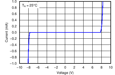 Figure 1. IV Curve
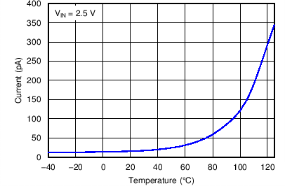 Figure 3. ILEAK vs Temperature
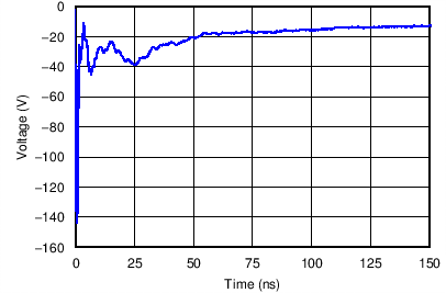 Figure 5. –8-kV Contact ESD Clamping
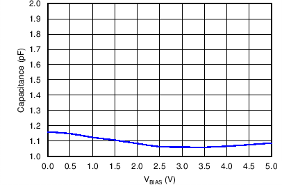 Figure 7. Capacitance vs VBIAS
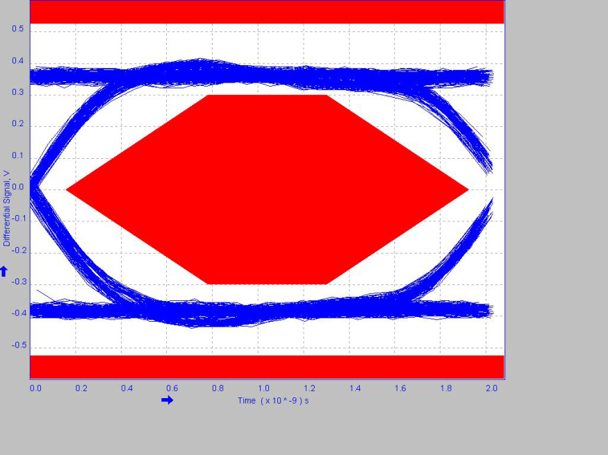 Figure 9. Eye Diagram With TPD2E1B06DRL on EVM
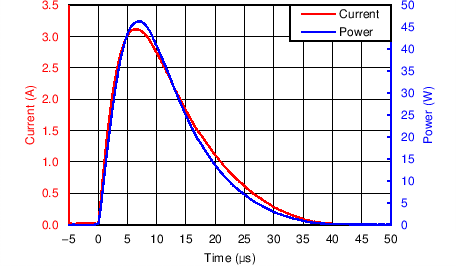 Figure 2. Maximum Surge Rating
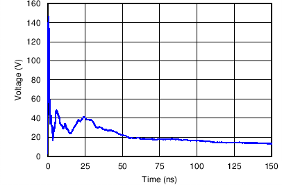 Figure 4. +8-kV Contact ESD Clamping
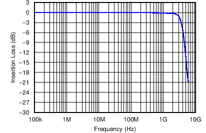 Figure 6. Insertion Loss
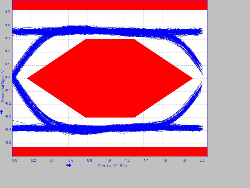 Figure 8. Eye Diagram Without TPD2E1B06DRL on EVM