SLLS949C September 2009 – January 2023 TPD2S017
PRODUCTION DATA
- 1 Features
- 2 Applications
- 3 Description
- 4 Revision History
- 5 Pin Configuration and Functions
- 6 Specifications
- 7 Detailed Description
- 8 Application and Implementation
- 9 Power Supply Recommendations
- 10Layout
- 11Device and Documentation Support
- 12Mechanical, Packaging, and Orderable Information
Package Options
Mechanical Data (Package|Pins)
- DBV|6
Thermal pad, mechanical data (Package|Pins)
Orderable Information
6.7 Typical Characteristics
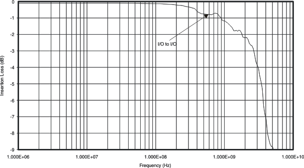 Figure 6-1 Insertion Loss Data (S21)
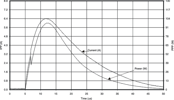
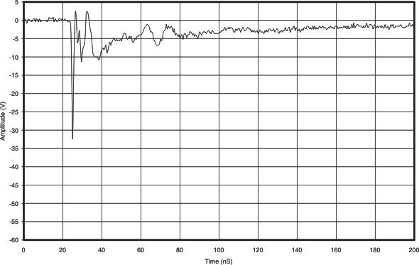 Figure 6-5 IEC Clamping Waveforms –8
kV Contact, 1 GHz Bandwidth
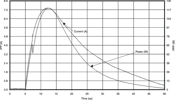 Figure 6-2 Peak Pulse Waveforms Ch1_Out, PUT with respect to GND, VCC = 5 V
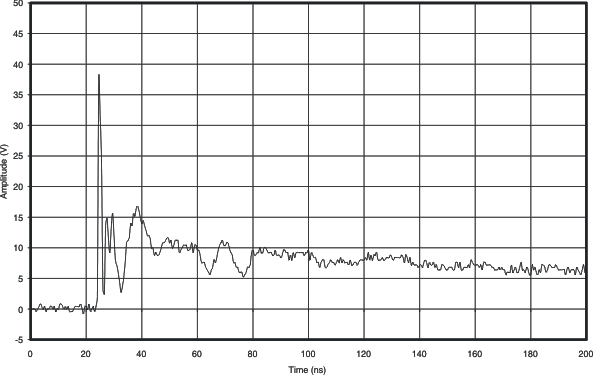 Figure 6-4 IEC Clamping Waveforms 8
kV Contact, 1 GHz Bandwidth