SLVSBR1F January 2013 – January 2015 TPD4S214
PRODUCTION DATA.
- 1 Features
- 2 Applications
- 3 Description
- 4 Simplified Schematic
- 5 Revision History
- 6 Pin Configuration and Functions
-
7 Specifications
- 7.1 Absolute Maximum Ratings
- 7.2 ESD Ratings
- 7.3 Recommended Operating Conditions
- 7.4 Thermal Information
- 7.5 Thermal Shutdown
- 7.6 Electrical Characteristics for EN, FLT, DET, D+, D-, VBUS, ID Pins
- 7.7 Electrical characteristics for UVLO / OVLO
- 7.8 Electrical Characteristics for DET Circuits
- 7.9 Electrical Characteristics for OTG Switch
- 7.10 Electrical Characteristics for Current Limit and Short Circuit Protection
- 7.11 Supply Current Consumption
- 7.12 Typical Characteristics
-
8 Detailed Description
- 8.1 Overview
- 8.2 Functional Block Diagram
- 8.3
Feature Description
- 8.3.1 Input Voltage Protection at VBUS from -7 V to 30 V
- 8.3.2 IEC 61000-4-2 Level 4 ESD Protection
- 8.3.3 Low RDS(ON) N-CH FET Switch for High Efficiency
- 8.3.4 Compliant with USB2.0 and USB3.0 OTG spec
- 8.3.5 User Adjustable Current Limit From 250 mA to Beyond 1.2 A
- 8.3.6 Built-in Soft-start
- 8.3.7 Reverse Current Blocking
- 8.3.8 Over Voltage Lock Out for VBUS
- 8.3.9 Under Voltage Lock Out for VOTG_IN
- 8.3.10 Thermal Shutdown and Short Circuit Protection
- 8.3.11 Auto Retry on any Fault; no Latching off States
- 8.3.12 Integrated VBUS Detection Circuit
- 8.3.13 Low Capacitance TVS ESD Clamp for USB2.0 High Speed Data Rate
- 8.3.14 Internal 16ms Startup Delay
- 8.3.15 Space Saving WCSP (12-YFF) Package
- 8.3.16 Inrush Current Protection
- 8.3.17 Input Capacitor (Optional)
- 8.3.18 Output Capacitor (Optional)
- 8.3.19 Current Limit
- 8.3.20 Thermal Shutdown
- 8.3.21 VBUS Detection
- 8.3.22 Test Configuration
- 8.4 Device Functional Modes
- 9 Application and Implementation
- 10Power Supply Recommendations
- 11Layout
- 12Device and Documentation Support
- 13Mechanical, Packaging, and Orderable Information
Package Options
Mechanical Data (Package|Pins)
- YFF|12
Thermal pad, mechanical data (Package|Pins)
Orderable Information
6 Pin Configuration and Functions
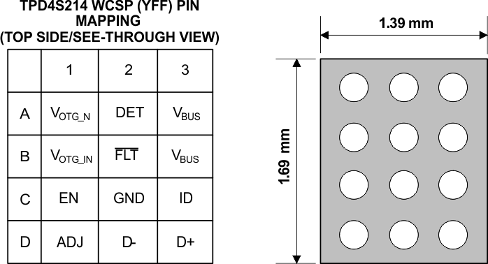
Pin Functions
| NAME | PIN | TYPE | DESCRIPTION | |
|---|---|---|---|---|
| D– | D2 | I/O | USB data– | |
| D+ | D3 | I/O | USB data+ | |
| ID | C3 | I/O | USB ID signal | |
| FLT | B2 | O | Open-Drain Output. Connect a pull-up resistor from FLT to the supply voltage of the host system. | |
| ADJ | D1 | I | Attach external resistor to adjust the current limit | |
| EN | C1 | I | Enable Input. Drive EN high to enable the OTG switch. | |
| VBUS | A3, B3 | O | USB Power Output | |
| VOTG_IN | A1, B1 | I | USB OTG Supply Input | |
| DET | A2 | O | Open-Drain Output. Connect a pull-up resistor from DET to the supply voltage of the host system. | |
| GND | C2 | Ground | Connect to PCB ground plane | |