SLVSBP3C December 2012 – May 2015 TPD5S116
PRODUCTION DATA.
- 1 Features
- 2 Applications
- 3 Description
- 4 Simplified Schematic
- 5 Revision History
- 6 Pin Configuration and Functions
-
7 Specifications
- 7.1 Absolute Maximum Ratings
- 7.2 ESD Ratings
- 7.3 Recommended Operating Conditions
- 7.4 Thermal Information
- 7.5 Electrical Characteristics
- 7.6 Voltage Level Shifter, SCL, SDA Lines
- 7.7 Voltage Level Shifter, CEC Line
- 7.8 Voltage Level Shifter, HPD Line
- 7.9 EN
- 7.10 Utility Pin
- 7.11 I/O Capacitances
- 7.12 Dynamic Load Characteristics
- 7.13 SCL, SDA Lines, VCCA = 1.2 V
- 7.14 CEC Line, VCCA = 1.2 V
- 7.15 HPD Line, VCCA = 1.2 V
- 7.16 SCL, SDA Lines, VCCA = 1.5 V
- 7.17 CEC Line, VCCA = 1.5 V
- 7.18 HPD Line, VCCA = 1.5 V
- 7.19 SCL, SDA Lines, VCCA = 1.8 V
- 7.20 CEC Line, VCCA = 1.8 V
- 7.21 HPD Line, VCCA = 1.8 V
- 7.22 SCL, SDA Lines, VCCA = 2.5 V
- 7.23 CEC Line, VCCA = 2.5 V
- 7.24 HPD Line, VCCA = 2.5 V
- 7.25 SCL, SDA Lines, VCCA = 3.3 V
- 7.26 CEC Line, VCCA = 3.3 V
- 7.27 HPD Line, VCCA = 3.3 V
- 7.28 SCL, SDA Lines, VCCA = 5 V
- 7.29 CEC Line, VCCA = 5 V
- 7.30 HPD Line, VCCA = 5 V
- 7.31 Typical Characteristics
-
8 Detailed Description
- 8.1 Overview
- 8.2 Functional Block Diagram
- 8.3
Feature Description
- 8.3.1 IEC 61000-4-2 Level 4 ESD Protection
- 8.3.2 Conforms to HDMI Control and 5VOUT Compliance Tests Without External Components
- 8.3.3 Auto-direction Sensing I2C Level Shifter with One-Shot Circuit to Drive Long HDMI Cable (750-pF Load)
- 8.3.4 Back Drive Protection
- 8.3.5 55-mA Load Switch with Short Circuit Protection
- 8.3.6 Hot Plug Detect Module with Pull Down Resistor
- 8.3.7 Integrated Pull-up and Pull-down Resistors per HDMI Specification
- 8.3.8 Utility Pin ESD Protection for Ethernet and Audio Return
- 8.3.9 DDC/CEC LEVEL SHIFT Circuit Operation
- 8.3.10 DDC/CEC Level Shifter Operational Notes For VCCA = 1.8V
- 8.3.11 Rise-Time Accelerators
- 8.3.12 Noise Considerations
- 8.3.13 HDMI Compliance
- 8.4 Device Functional Modes
- 9 Applications and Implementations
- 10Power Supply Requirements
- 11Layout
- 12Device and Documentation Support
- 13Mechanical, Packaging, and Orderable Information
Package Options
Mechanical Data (Package|Pins)
- YFF|15
Thermal pad, mechanical data (Package|Pins)
Orderable Information
10 Power Supply Requirements
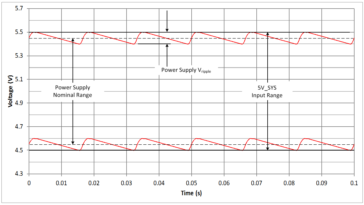
TPD5S116 has two power input pins: 5V_SYS and VCCA. It can operate normally with 5V_SYS between 4.5 V and 5.5 V; and VCCA between 1.1 V and 5.5 V. Thus, the power supply (with a ripple of VRIPPLE) requirement for TPD5S116 for 5V_SYS is between 4.5 V + ½VRIPPLE and 5.5 V – ½VRIPPLE; and for VCCA it is between 1.1 V + ½VRIPPLE and 5.5 V – ½VRIPPLE.
 Figure 21. Power Supply Ripple and TPD5S116 5V_SYS Voltage Requirements