SLIS125B December 2006 – December 2014 TPIC74100-Q1
PRODUCTION DATA.
- 1 Features
- 2 Applications
- 3 Description
- 4 Revision History
- 5 Pin Configuration and Functions
- 6 Specifications
-
7 Detailed Description
- 7.1 Overview
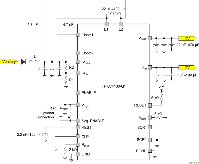
- 7.2 Functional Block Diagram
- 7.3
Feature Description
- 7.3.1 Switch-Mode Input/Output Pins (L1, L2)
- 7.3.2 Supply Pin (Vdriver)
- 7.3.3 Internal Supply Decoupling Pin (Vlogic)
- 7.3.4 Input Voltage Monitoring Pin (AIN)
- 7.3.5 Input Undervoltage Alarm Pin (AOUT)
- 7.3.6 Reset Delay Timer Pin (REST)
- 7.3.7 Reset Pin (RESET)
- 7.3.8 Main Regulator Output Pin (VOUT)
- 7.3.9 Low-Power-Mode Pin (CLP)
- 7.3.10 Switch-Output Pin (5Vg)
- 7.3.11 5Vg-Enable Pin (5Vg_ENABLE)
- 7.3.12 Slew-Rate Control Pins (SCR0, SCR1)
- 7.3.13 Modulator Frequency Setting (Pin Rmod)
- 7.3.14 Ground Pin (PGND)
- 7.3.15 Enable Pin (ENABLE)
- 7.3.16 Bootstrap Pins (Cboot1 and Cboot2)
- 7.4 Device Functional Modes
- 8 Applications and Implementation
- 9 Power Supply Recommendations
- 10Layout
- 11Device and Documentation Support
- 12Mechanical, Packaging, and Orderable Information
Package Options
Mechanical Data (Package|Pins)
- PWP|20
Thermal pad, mechanical data (Package|Pins)
- PWP|20
Orderable Information
8 Applications and Implementation
NOTE
Information in the following applications sections is not part of the TI component specification, and TI does not warrant its accuracy or completeness. TI’s customers are responsible for determining suitability of components for their purposes. Customers should validate and test their design implementation to confirm system functionality.
8.1 Application Information
The TPIC74100-Q1 is a switch-mode regulator with integrated switches for voltage-mode control. With the help of external LC components, the device regulates the output to 5 V +-3% for a wide input voltage range. The device can monitor the output voltage as well as the input voltage.
8.2 Typical Application
8.2.1 Design Requirements
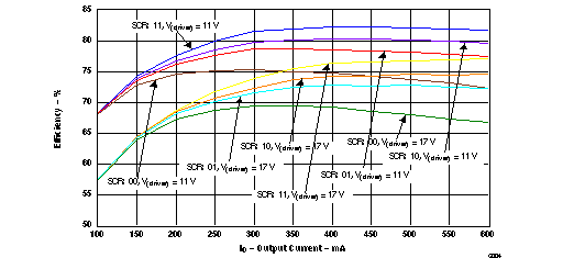
Plot the converter efficiency with four different slew rate controls (SCRx) at an input voltage of 11 V and 17 V. The slew rate of the switching transistor Q1 can be changed using the SCR0 and SCR1 pins.
8.2.2 Detailed Design Procedure
8.2.2.1 Buck Mode
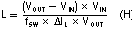
- Select inductor ripple current ΔIL: for example ΔIL = 0.2 × IOUT
- Calculate inductor L
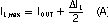
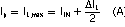
- Inductor peak current
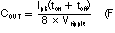
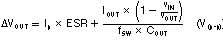
- Output voltage ripple
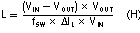
where fSW is the regulator switching frequency.
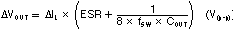
Usually, the first term is dominant.
8.2.2.2 Boost Mode
- Select inductor ripple current ΔIL: for example ΔIL = 0.2 × IIN
- Calculate inductor L
- Inductor peak current
- Output voltage ripple
where fSW is the regulator switching frequency.
8.2.3 Application Curve