SLIS144B September 2011 – February 2017
PRODUCTION DATA.
- 1 Features
- 2 Applications
- 3 Description
- 4 Revision History
- 5 Device Comparison Table
- 6 Pin Configuration and Functions
- 7 Specifications
- 8 Parameter Measurement Information
- 9 Detailed Description
- 10Application and Implementation
- 11Power Supply Recommendations
- 12Layout
- 13Device and Documentation Support
- 14Mechanical, Packaging, and Orderable Information
Package Options
Mechanical Data (Package|Pins)
- DCK|6
Thermal pad, mechanical data (Package|Pins)
- DCK|6
Orderable Information
10 Application and Implementation
10.1 Application Information
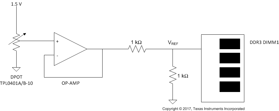
There are many applications in which voltage division is needed through the use of a digital potentiometer such as the TPL0401x-10; this is one example of the many. In conjunction with many amplifiers, the TPL0401x-10 can effectively be used in voltage divider mode to create a buffer to adjust the reference voltage for DDR3 DIMM1 Memory.
10.2 Typical Application
 Figure 20. DDR3 Voltage Reference Adjustment
10.2.1 Design Requirements
Table 3 lists the design parameters for this example.
Table 3. Design Parameters
| PARAMETER | EXAMPLE VALUE |
|---|---|
| Input voltage | 1.5 V |
| VREF | 0 V to 0.75 V |
10.2.2 Detailed Design Procedure
The TPL0401x-10 can be used in voltage divider mode with a unity-gain op amp buffer to provide a clean voltage reference for DDR3 DIMM1 Memory. The analog output voltage, VREF1 is determined by the wiper setting programmed through the I2C bus.
The op amp is required to buffer the high-impedance output of the TPL0401x-10 or else loading placed on the output of the voltage divider affects the output voltage.
10.2.3 Application Curve
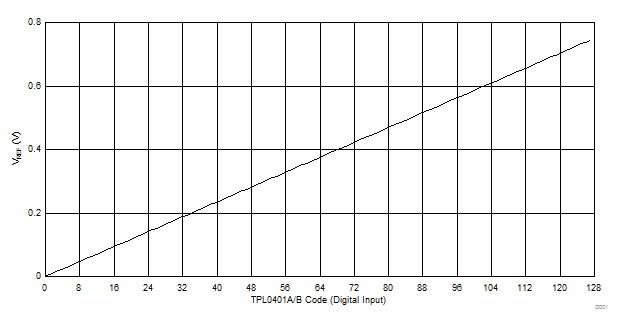
The voltage, 1.5 V, applied to terminal H of TPL0401x-10 determines the voltage that is buffered by the unity-gain op amp and divided as the DDR3 DIMM1 voltage reference. By using the TPL0401x-10, and dividing the 1.5 V, a maximum of 0.75 V is applied to the buffer and passed to the voltage divider. The output voltage then ranges from 0 V to 0.75 V.
 Figure 21. TPL0401-10 Digital Input vs Reference Voltage for DDR3 DIMM Memory