SLVSET9F September 2018 – February 2023 TPS1663
PRODUCTION DATA
- 1 Features
- 2 Applications
- 3 Description
- 4 Revision History
- 5 Device Comparison Table
- 6 Pin Configuration and Functions
- 7 Specifications
- 8 Parameter Measurement Information
-
9 Detailed Description
- 9.1 Overview
- 9.2 Functional Block Diagram
- 9.3
Feature Description
- 9.3.1 Hot Plug-In and In-Rush Current Control
- 9.3.2 Undervoltage Lockout (UVLO)
- 9.3.3 Overvoltage Protection (OVP)
- 9.3.4 Overload and Short Circuit Protection
- 9.3.5 Output Power Limiting, PLIM (TPS16632 Only)
- 9.3.6 Current Monitoring Output (IMON)
- 9.3.7 FAULT Response (FLT)
- 9.3.8 Power Good Output (PGOOD)
- 9.3.9 IN, P_IN, OUT and GND Pins
- 9.3.10 Thermal Shutdown
- 9.3.11 Low Current Shutdown Control (SHDN)
- 9.4 Device Functional Modes
- 10Application and Implementation
- 11Device and Documentation Support
- 12Mechanical, Packaging, and Orderable Information
Package Options
Refer to the PDF data sheet for device specific package drawings
Mechanical Data (Package|Pins)
- RGE|24
- PWP|20
Thermal pad, mechanical data (Package|Pins)
Orderable Information
3 Description
The TPS1663x is an easy-to-use, positive 60-V, 6-A eFuse with a 31-mΩ integrated FET. Protection for the load, source, and eFuse itself are provided along with adjustable features such as accurate overcurrent protection, fast short circuit protection, output slew rate control, overvoltage protection and undervoltage lockout. The TPS16332 device integrates adjustable output power limiting (PLIM) functionality that simplifies and enables compliance to standards such as IEC61010-1 and UL1310. The device also includes adjustable overcurrent functionality. PGOOD can be used for enable and disable control of the downstream DC/DC converters.
A shutdown pin provides external control for enabling and disabling the internal FET, as well as placing the device in a low current shutdown mode. For system status monitoring and downstream load control, the device provides fault and a precise current monitor output. The MODE pin allows flexibility to configure the device between the two current-limiting fault responses (latch off and auto-retry).
The devices are available in a 4-mm × 4-mm 24-pin VQFN package and are specified over a –40°C to +125°C temperature range.
| PART NUMBER | PACKAGE(1) | BODY SIZE (NOM) |
|---|---|---|
| TPS16630 TPS16632 |
VQFN (24) | 4.00 mm × 4.00 mm |
| TPS16630 | HTSSOP (20) | 6.50 mm × 4.40 mm |
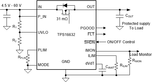
 Simplified Schematic
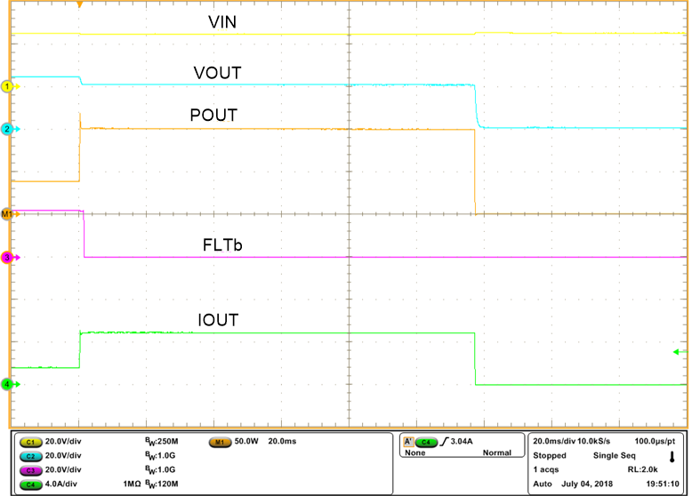
 Output Power Limiting Performance of
TPS16632