SLVSCM2D October 2014 – December 2019 TPS1H100-Q1
PRODUCTION DATA.
- 1 Features
- 2 Applications
- 3 Description
- 4 Revision History
- 5 Pin Configuration and Functions
- 6 Specifications
-
7 Detailed Description
- 7.1 Overview
- 7.2 Functional Block Diagram
- 7.3
Feature Description
- 7.3.1 Accurate Current Sense
- 7.3.2 Programmable Current Limit
- 7.3.3 Inductive-Load Switching-Off Clamp
- 7.3.4
Full Protections and Diagnostics
- 7.3.4.1 Short-to-GND and Overload Detection
- 7.3.4.2 Open-Load Detection
- 7.3.4.3 Short-to-Battery Detection
- 7.3.4.4 Reverse-Polarity Detection
- 7.3.4.5 Thermal Protection Behavior
- 7.3.4.6 UVLO Protection
- 7.3.4.7 Loss of GND Protection
- 7.3.4.8 Loss of Power Supply Protection
- 7.3.4.9 Reverse Current Protection
- 7.3.4.10 Protection for MCU I/Os
- 7.3.5 Diagnostic Enable Function
- 7.4 Device Functional Modes
- 8 Application and Implementation
- 9 Power Supply Recommendations
- 10Layout
- 11Device and Documentation Support
- 12Mechanical, Packaging, and Orderable Information
Package Options
Mechanical Data (Package|Pins)
- PWP|14
Thermal pad, mechanical data (Package|Pins)
- PWP|14
Orderable Information
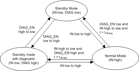
7.4.1 Working Mode
The three working modes in the device are normal mode, standby mode, and standby mode with diagnostic. If an off-state power saving is required in the system, the standby current is less than 500 nA with DIAG_EN low. If an off-state diagnostic is required in the system, the typical standby current is around 1 mA with DIAG_EN high. Note that to enter standby mode requires IN low and t > toff,deg. toff,deg is the standby-mode deglitch time, which is used to avoid false triggering. Figure 44 shows a work-mode state-machine state diagram.
 Figure 44. Work-Mode State Machine