SLVSEE0D February 2018 – September 2021 TPS1H200A-Q1
PRODUCTION DATA
- 1 Features
- 2 Applications
- 3 Description
- 4 Revision History
- 5 Pin Configuration and Functions
- 6 Specifications
- 7 Detailed Description
- 8 Application and Implementation
- 9 Power Supply Recommendations
- 10Layout
- 11Device and Documentation Support
- 12Mechanical, Packaging, and Orderable Information
Package Options
Mechanical Data (Package|Pins)
- DGN|8
Thermal pad, mechanical data (Package|Pins)
- DGN|8
Orderable Information
7.3.1 Current limit
A high-accuracy current limit allows high reliability of the design. The current limit protects the load and the power supply from overstressing during short-circuit-to-GND or power-up conditions. The current limit can also save system cost by reducing the size of PCB traces and connectors, and the capacity of the preceding power stage.
When a current limit threshold is hit, a closed loop immediately activates. The output current is clamped at the set value, and a fault is reported. The device heats up because of high power dissipation on the power FET.
The device has two current limit thresholds.
Internal current limit: The internal current limit is fixed at ICL(int). Tie the CL pin directly to the device GND for large-transient-current applications.
External adjustable current limit: An external resistor is used to set the current limit threshold. Use Equation 1 to calculate R(CL). The external adjustable current limit allows the flexibility to set the current limit value by application.
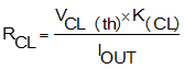
where
- VCL(th) is the internal band-gap voltage.
- K(CL) is the ratio of the output current and the current limit set value.
- K(CL) is constant across temperature and supply voltage.
When a GND network is used, that causes a level shift between the device GND and board GND, so the CL pin must be connected to the device GND.
For better protection from a hard short-to-GND condition (when the IN pin is enabled, a short-to-GND occurs suddenly), the device will implement a fast-trip protection to turn off the output before the current limit closed loop is set up. Typically, the fast-trip response time is less than 1 µs. With a fast response like this, the device can achieve a better inrush current-suppression performance.
 Figure 7-1 Current Limit