SLVS514N june 2010 – july 2023 TPS2041B , TPS2042B , TPS2043B , TPS2044B , TPS2051B , TPS2052B , TPS2053B , TPS2054B
PRODUCTION DATA
- 1
- 1 Features
- 2 Applications
- 3 Description
- 4 Revision History
- 5 General Switch Catalog
- 6 Pin Configuration and Functions
- 7 Specifications
- 8 Parameter Measurement Information
- 9 Detailed Description
- 10Application and Implementation
- 11Power Supply Recommendations
- 12Layout
- 13Device and Documentation Support
- 14Mechanical, Packaging, and Orderable Information
Package Options
Mechanical Data (Package|Pins)
- D|16
Thermal pad, mechanical data (Package|Pins)
- D|16
Orderable Information
3 Description
The TPS20xxB power-distribution switches are intended for applications where heavy capacitive loads and short circuits are likely to be encountered. These devices incorporates 70-mΩ N-channel MOSFET power switches for power-distribution systems that require multiple power switches in a single package. Each switch is controlled by a logic enable input. Gate drive is provided by an internal charge pump designed to control the power-switch rise times and fall times to minimize current surges during switching. The charge pump requires no external components and allows operation from supplies as low as 2.7 V.
When the output load exceeds the current-limit threshold or a short is present, the device limits the output current to a safe level by switching into a constant-current mode, pulling the overcurrent ( OCx) logic output low. When continuous heavy overloads and short circuits increase the power dissipation in the switch, causing the junction temperature to rise, a thermal protection circuit shuts off the switch to prevent damage. Recovery from a thermal shutdown is automatic once the device has cooled sufficiently. Internal circuitry ensures that the switch remains off until valid input voltage is present. This power-distribution switch is designed to set current limit at 1 A (typical).
| PART NUMBER | PACKAGE(1) | BODY SIZE (NOM) |
|---|---|---|
| TPS20xxB | SOIC (8) | 4.90 mm × 3.91 mm |
| SOIC (16) | 9.90 mm × 3.91 mm | |
| SOT-23 (5) | 2.90 mm × 1.60 mm | |
| HVSSOP (8) | 3.00 mm × 3.00 mm | |
| SON (8) | 3.00 mm × 3.00 mm |
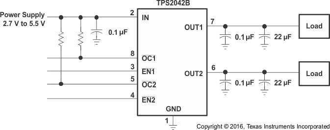
 Typical Application Schematic