SLVSFG1A January 2021 – May 2021 TPS2116
PRODUCTION DATA
- 1 Features
- 2 Applications
- 3 Description
- 4 Revision History
- 5 Pin Configuration and Functions
- 6 Specifications
- 7 Detailed Description
- 8 Application and Implementation
- 9 Power Supply Recommendations
- 10Layout
- 11Device and Documentation Support
- 12Mechanical, Packaging, and Orderable Information
Package Options
Mechanical Data (Package|Pins)
- DRL|8
Thermal pad, mechanical data (Package|Pins)
Orderable Information
7.6.1 Priority/Manual Mode
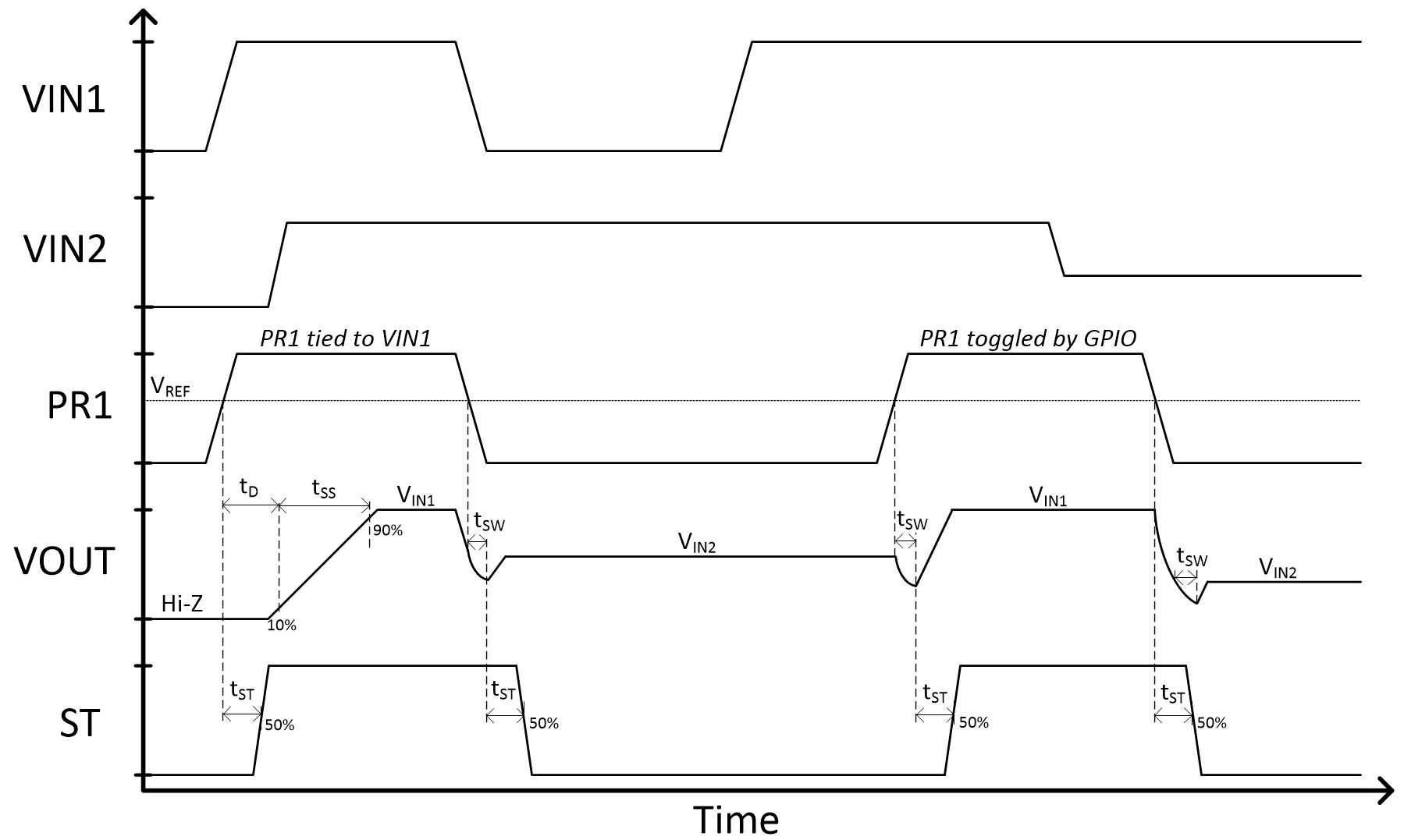
When MODE is tied high, PR1 determines the channel selected. To configure VIN1 as the priority supply, connect MODE to VIN1 and set the proper threshold through a resistor divider from VIN1 to PR1. To configure manual selection, pull up MODE to an external supply and follow the truth table. When PR1 is pulled above VREF, the voltage on VIN1 is used to power the output, and when it is pulled below VREF, VIN2 is used to power the output. The expected behavior for the device is shown in the waveform below.
 Figure 7-2 Priority/Manual Mode Switching
When PR1 is toggled, the device implements a break-before-make switchover which shuts off both channels before turning on the new channel to power the output. This means that for time tSW, the output is unpowered and will dip depending on the load current and output capacitance. If the output voltage is greater than the input supply being switched to, then the device will not turn on the new channel until the output has discharged down to VIN + VRCB to prevent reverse current flow.
When MODE is pulled low and PR1 is pulled high, the device enters shutdown. Both channels are turned off and the output is high impedance. When the PR1 pin is pulled low, the higher voltage supply between VIN1 and VIN2 is passed to the output.