SLVS914E April 2009 – April 2024 TPS22960
PRODUCTION DATA
- 1
- 1 Features
- 2 Applications
- 3 Description
- 4 Pin Configuration and Functions
- 5 Specifications
- 6 Parameter Measurement Information
- 7 Detailed Description
- 8 Application and Implementation
- 9 Device and Documentation Support
- 10Revision History
- 11Mechanical, Packaging, and Orderable Information
Package Options
Mechanical Data (Package|Pins)
Thermal pad, mechanical data (Package|Pins)
- DCN|8
Orderable Information
3 Description
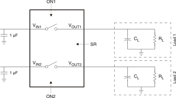
The TPS22960 is a small low-rON dual-channel load switch with controlled turnon. The devices contain two P-channel MOSFETs that can operate over an input voltage range of 1.62V to 5.5V. Each switch is independently controlled by on/off inputs (ON1 and ON2), which are capable of interfacing directly with low-voltage control signals. In TPS22960 a 85Ω on-chip load resistor is added for quick discharge when the switch is turned off.
The rise time (slew-rate) of the device is internally controlled in order to avoid inrush current, and it can be slowed down if needed using the SR pin: at 3.3V, TPS22960 features a 75μs rise time with the SR pin tied to ground and 660μs with the SR pin tied to high.
The TPS22960 is available in a space-saving 8-pin UQFN package and in an 8-pin SOT package. It is characterized for operation over the free-air temperature range of –40°C to 85°C.
| PART NUMBER | PACKAGE(1) | PACKAGE SIZE(2) |
|---|---|---|
| TPS22960 | DCN (SOT, 8) | 2.90mm × 1.63mm |
| RSE (UQFN, 8) | 1.50mm × 1.50mm |
 Simplified Diagram