SLVSBS6A June 2013 – January 2015 TPS22963C , TPS22964C
PRODUCTION DATA.
- 1 Features
- 2 Applications
- 3 Description
- 4 Simplified Schematic
- 5 Revision History
- 6 Device Comparison Table
- 7 Pin Configuration and Functions
- 8 Specifications
- 9 Parametric Measurement Information
- 10Detailed Description
- 11Application and Implementation
- 12Power Supply Recommendations
- 13Layout
- 14Device and Documentation Support
- 15Mechanical, Packaging, and Orderable Information
Package Options
Mechanical Data (Package|Pins)
- YZP|6
Thermal pad, mechanical data (Package|Pins)
Orderable Information
11 Application and Implementation
NOTE
Information in the following applications sections is not part of the TI component specification, and TI does not warrant its accuracy or completeness. TI’s customers are responsible for determining suitability of components for their purposes. Customers should validate and test their design implementation to confirm system functionality.
11.1 Application Information
11.1.1 Input Capacitor
It is recommended to place a capacitor (CIN) between VIN and GND pins of TPS22963/64. This capacitor helps to limit the voltage drop on the input voltage supply when the switch turns ON into a discharged load capacitor. A 1-µF ceramic capacitor that is placed close to the IC pins is usually sufficient. Higher values of CIN can be used to further reduce the voltage drop in high current applications.
11.1.2 Output Capacitor
It is recommended to place a capacitor (COUT) between VOUT and GND pins of TPS22963/64. This capacitor acts as a low pass filter along with the switch ON-resistance to remove any voltage glitches coming from the input voltage source. It is generally recommended to have CIN greater than COUT so that once the switch is turned ON, COUT can charge up to VIN without VIN dropping significantly. A 0.1-µF ceramic capacitor that is placed close to the IC pins is usually sufficient.
11.1.3 Standby Power Reduction
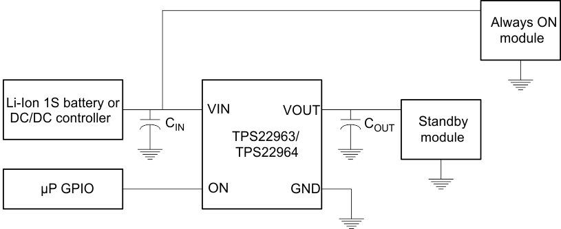 Figure 38. Standby Power Reduction
Any end equipment that is being powered from the battery has a need to reduce current consumption in order to keep the battery charged for a longer time. TPS22963/64 helps to accomplish this by turning off the supply to the modules that are in standby state and hence significantly reduces the leakage current overhead of the standby modules.
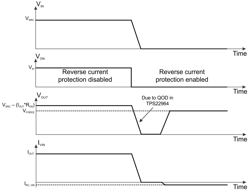
11.1.4 Reverse Current Protection
The reverse current protection feature prevents the current to flow from VOUT to VIN when TPS22963/64 is disabled. This feature is particularly useful when the output of TPS22963/64 needs to be driven by another voltage source after TPS22963/64 is disabled (for example in a power multiplexer application). In order for this feature to work, TPS22963/64 has to be disabled and either of the following conditions shall be met: VIN > 1 V or VOUT > 1 V.
Figure 39 demonstrates the ideal behavior of reverse current protection circuit in TPS22963/64. After the device is disabled via the ON pin and VOUT is forced to an external voltage VFORCE, a very small amount of current given by IRC,VIN will flow from VOUT to VIN. This will prevent any extra current loading on the voltage source supplying the VFORCE voltage.
11.1.5 Power Supply Sequencing Without a GPIO Input
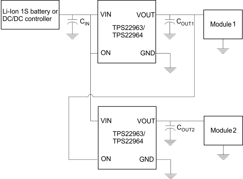 Figure 40. Power Supply Sequencing Without a GPIO Input
In many end equipments, there is a need to power up various modules in a pre-determined manner. TPS22963/64 can solve the problem of power sequencing without adding any complexity to the overall system. Figure 40 shows the configuration required for powering up two modules in a fixed sequence. The output of the first load switch is tied to the enable of the second load switch, so when Module 1 is powered the second load switch is enabled and Module 2 is powered.
11.2 Typical Application
TPS22963/64 is an ultra-low ON-resistance, 3-A integrated load switch that is capable of interfacing directly with 1S battery in portable consumer devices such as smartphones, tablets etc. Its wide input voltage range (1 V to 5.5 V) makes it suitable to be used for lower voltage rails as well inside different end equipments to accomplish power sequencing, inrush current control and reducing leakage current in sub-systems that are in standby mode. Figure 41 shows the typical application circuit of TPS22963/64.
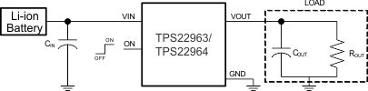 Figure 41. Typical Application Circuit
11.2.1 Design Requirements
| DESIGN PARAMETER | EXAMPLE VALUE |
|---|---|
| VIN | 3.3 V |
| CL | 4.7 µF |
| Maximum Acceptable Inrush Current | 30 mA |
11.2.2 Detailed Design Procedure
11.2.2.1 Managing Inrush Current
When the switch is enabled, the output capacitors must be charged up from 0 V to the set value (3.3 V in this example). This charge arrives in the form of inrush current. Inrush current can be calculated using the following equation:

where
- C = output capacitance
- dV = output voltage
- dt = rise time
The TPS22963/64 offers a controlled rise time for minimizing inrush current. This device can be selected based upon the minimum acceptable rise time which can be calculated using the design requirements and the inrush current equation. An output capacitance of 4.7 µF will be used since the amound of inrush current increases with output capacitance:
To ensure an inrush current of less than 30 mA, a device with a rise time greater than 517 µs must be used. The TPS22963/64 has a typical rise time of 715 µs at 3.3 V which meets the above design requirements.
11.2.3 Application Curves
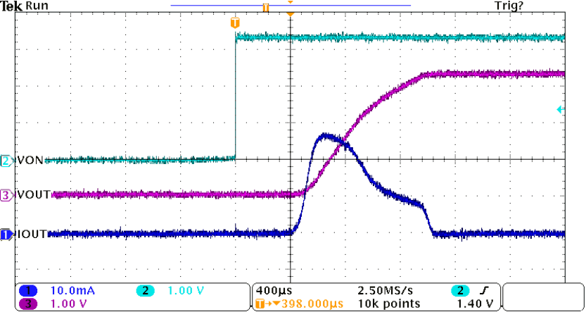 Figure 42. TPS22963/64 Inrush Current with 4.7 µF Output Capacitor