SLVSDK7C April   2017  – February 2020 TPS22971

PRODUCTION DATA.  

  1. Features
  2. Applications
  3. Description
    1.     Device Images
      1.      Typical Application
  4. Revision History
  5. Pin Configuration and Functions
    1.     Pin Functions
  6. Specifications
    1. 6.1 Absolute Maximum Ratings
    2. 6.2 ESD Ratings
    3. 6.3 Recommended Operating Conditions
    4. 6.4 Thermal Information
    5. 6.5 Electrical Characteristics
    6. 6.6 Switching Characteristics
    7. 6.7 Typical DC Characteristics
    8. 6.8 Typical AC Characteristics
  7. Parameter Measurement Information
  8. Detailed Description
    1. 8.1 Overview
    2. 8.2 Functional Block Diagram
    3. 8.3 Feature Description
      1. 8.3.1 On and Off Control
      2. 8.3.2 Controlled Turn-On
      3. 8.3.3 Power Good (PG)
      4. 8.3.4 Quick Output Discharge (QOD)
    4. 8.4 Device Functional Modes
  9. Application and Implementation
    1. 9.1 Application Information
      1. 9.1.1 Thermal Consideration
      2. 9.1.2 PG Pull Up Resistor
      3. 9.1.3 Power Sequencing
    2. 9.2 Typical Application
      1. 9.2.1 Design Requirements
      2. 9.2.2 Detailed Design Procedure
        1. 9.2.2.1 Maximum Voltage Drop and On-Resistance
        2. 9.2.2.2 Managing Inrush Current
      3. 9.2.3 Application Curves
  10. 10Power Supply Recommendations
  11. 11Layout
    1. 11.1 Layout Guidelines
    2. 11.2 Layout Example
  12. 12Device and Documentation Support
    1. 12.1 Documentation Support
      1. 12.1.1 Related Documentation
    2. 12.2 Receiving Notification of Documentation Updates
    3. 12.3 Community Resources
    4. 12.4 Trademarks
    5. 12.5 Electrostatic Discharge Caution
    6. 12.6 Glossary
  13. 13Mechanical, Packaging, and Orderable Information

Package Options

Mechanical Data (Package|Pins)
Thermal pad, mechanical data (Package|Pins)
Orderable Information

Pin Configuration and Functions

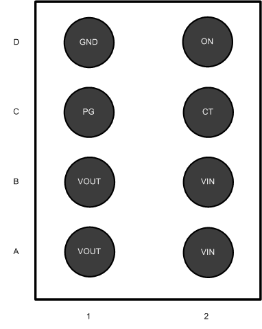
YZP Package
8-Pin DSBGA
Laser Marking View
TPS22971 PIN-Configuration-1.gif
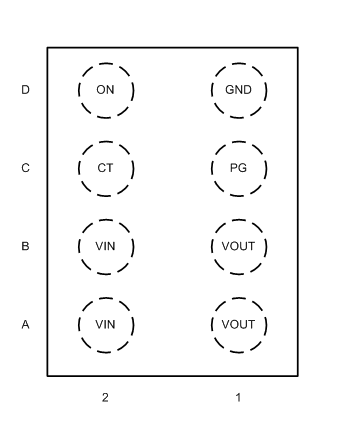
YZP Package
8-Pin DSBGA
Bump View
TPS22971 TPS22971_Pinout.gif

Pin Functions

PIN I/O DESCRIPTION
NAME NO.
CT C2 O VOUT slew rate control. Adding capacitance from this pin to ground lowers the output slew rate
GND D1 GND Ground
ON D2 I Switch enable control input. Do not leave floating
PG C1 O Power Good Indication. Open drain releases when the switch is fully on
VOUT A1, B1 O Switch output
VIN A2, B2 I Switch input