SLVS503F November   2003  – February 2020 TPS2490 , TPS2491

PRODUCTION DATA.  

  1. Features
  2. Applications
  3. Description
    1.     Device Images
      1.      Typical Application
  4. Revision History
  5. Pin Configuration and Functions
    1.     Pin Functions
  6. Specifications
    1. 6.1 Absolute Maximum Ratings
    2. 6.2 ESD Ratings
    3. 6.3 Recommended Operating Conditions
    4. 6.4 Thermal Information
    5. 6.5 Electrical Characteristics
    6. 6.6 Switching Characteristics
    7. 6.7 Typical Characteristics
  7. Detailed Description
    1. 7.1 Overview
    2. 7.2 Functional Block Diagram
    3. 7.3 Feature Description
      1. 7.3.1  VCC
      2. 7.3.2  SENSE
      3. 7.3.3  GATE
      4. 7.3.4  OUT
      5. 7.3.5  EN
      6. 7.3.6  VREF
      7. 7.3.7  PROG
      8. 7.3.8  TIMER
      9. 7.3.9  PG
      10. 7.3.10 GND
    4. 7.4 Device Functional Modes
      1. 7.4.1 Board Plug-In ()
      2. 7.4.2 TIMER and PG Operation ()
      3. 7.4.3 Action of the Constant Power Engine ()
      4. 7.4.4 Response to a Hard Output Short ( and )
      5. 7.4.5 Automatic Restart ()
  8. Application and Implementation
    1. 8.1 Application Information
      1. 8.1.1 Alternative Inrush Designs
        1. 8.1.1.1 Gate Capacitor (dV/dt) Control
        2. 8.1.1.2 PROG Inrush Control
      2. 8.1.2 Additional Design Considerations
        1. 8.1.2.1 Use of PG
        2. 8.1.2.2 Faults and Backplane Voltage Droop
        3. 8.1.2.3 Output Clamp Diode
        4. 8.1.2.4 Gate Clamp Diode
        5. 8.1.2.5 High Gate Capacitance Applications
        6. 8.1.2.6 Input Bypass
        7. 8.1.2.7 Output Short Circuit Measurements
    2. 8.2 Typical Application
      1. 8.2.1 Design Requirements
      2. 8.2.2 Detailed Design Procedure
        1. 8.2.2.1 Select RSNS and CL setting
        2. 8.2.2.2 Selecting the Hot Swap FET(s)
        3. 8.2.2.3 Select Power Limit
        4. 8.2.2.4 Set Fault Timer
        5. 8.2.2.5 Check MOSFET SOA
        6. 8.2.2.6 Set Under-Voltage Threshold
        7. 8.2.2.7 Choose R5, and CIN
        8. 8.2.2.8 Input and Output Protection
        9. 8.2.2.9 Final Schematic and Component Values
      3. 8.2.3 Application Curves
  9. Power Supply Recommendations
  10. 10Layout
    1. 10.1 Layout Guidelines
      1. 10.1.1 PC Board Guidelines
      2. 10.1.2 System Considerations
    2. 10.2 Layout Example
  11. 11Device and Documentation Support
    1. 11.1 Development Support
    2. 11.2 Documentation Support
      1. 11.2.1 Related Documentation
    3. 11.3 Related Links
    4. 11.4 Receiving Notification of Documentation Updates
    5. 11.5 Community Resources
    6. 11.6 Trademarks
    7. 11.7 Electrostatic Discharge Caution
    8. 11.8 Glossary
  12. 12Mechanical, Packaging, and Orderable Information

Package Options

Refer to the PDF data sheet for device specific package drawings

Mechanical Data (Package|Pins)
  • DGS|10
Thermal pad, mechanical data (Package|Pins)
Orderable Information

Typical Application

This section describes the design procedure for a 24-V, 10-A hot swap design.
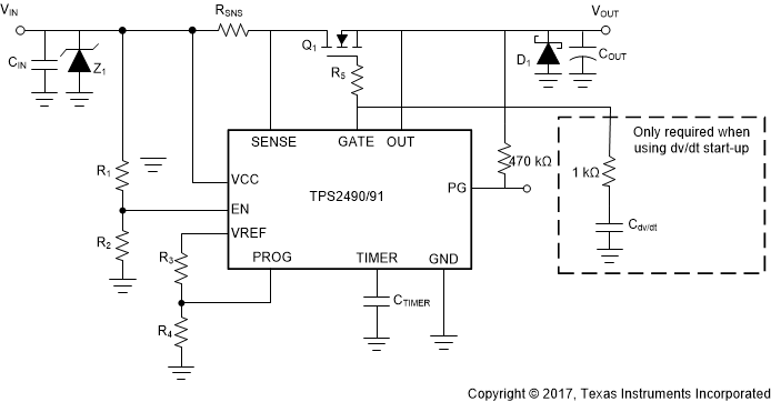
TPS2490 TPS2491 tps2490_typical_application_schemat.gifFigure 18. Typical Application Schematic, TPS2490