SLVSCJ0E March   2014  – June 2021 TPS25200

PRODUCTION DATA  

  1. Features
  2. Applications
  3. Description
  4. Revision History
  5. Pin Configuration and Functions
  6. Specifications
    1. 6.1 Absolute Maximum Ratings
    2. 6.2 ESD Ratings
    3. 6.3 Recommended Operating Conditions
    4. 6.4 Thermal Information
    5. 6.5 Electrical Characteristics
    6. 6.6 Timing Requirements
    7. 6.7 Typical Characteristics
  7. Parameter Measurement Information
  8. Detailed Description
    1. 8.1 Overview
    2. 8.2 Functional Block Diagram
    3. 8.3 Feature Description
      1. 8.3.1 Enable
      2. 8.3.2 Thermal Sense
      3. 8.3.3 Overcurrent Protection
      4. 8.3.4 FAULT Response
      5. 8.3.5 Output Discharge
    4. 8.4 Device Functional Modes
      1. 8.4.1 Undervoltage Lockout (UVLO)
      2. 8.4.2 Overcurrent Protection (OCP)
      3. 8.4.3 Overvoltage Clamp (OVC)
      4. 8.4.4 Overvoltage Lockout (OVLO)
  9. Application and Implementation
    1. 9.1 Application Information
    2. 9.2 Typical Application
      1. 9.2.1 Design Requirements
      2. 9.2.2 Detailed Design Procedure
        1. 9.2.2.1 Step by Step Design Produce
        2. 9.2.2.2 Input and Output Capacitance
        3. 9.2.2.3 Programming the Current-Limit Threshold
        4. 9.2.2.4 Design Above a Minimum Current Limit
        5. 9.2.2.5 Design Below a Maximum Current Limit
        6. 9.2.2.6 Power Dissipation and Junction Temperature
      3. 9.2.3 Application Curves
  10. 10Power Supply Recommendations
  11. 11Layout
    1. 11.1 Layout Guidelines
    2. 11.2 Layout Example
  12. 12Device and Documentation Support
    1. 12.1 Documentation Support
      1. 12.1.1 Related Documentation
    2. 12.2 Receiving Notification of Documentation Updates
    3. 12.3 Support Resources
    4. 12.4 Trademarks
    5. 12.5 Electrostatic Discharge Caution
    6. 12.6 Glossary
  13. 13Mechanical, Packaging, and Orderable Information

Package Options

Mechanical Data (Package|Pins)
Thermal pad, mechanical data (Package|Pins)
Orderable Information

Design Below a Maximum Current Limit

Some applications require that current limiting must occur below a certain threshold. For this example, assume that 2.9 A must be delivered to the load so that the minimum desired current-limit threshold is 2900 mA. Use the IOS equations (Equation 1) and Figure 9-5 to select RILIM as shown in Equation 5.

Equation 5. GUID-6727038C-721B-4FF7-B52A-E5AF6B7B9DF5-low.gif

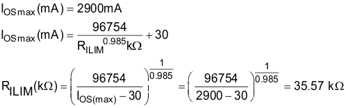
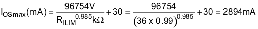
Select the closest 1% resistor greater than the calculated value: RILIM = 36 kΩ. This sets the maximum current-limit threshold at 2894 mA as shown in Equation 6.

Equation 6. GUID-F2E88ADE-A79E-40CB-811C-A4FAF2785764-low.gif

Use the IOS equations, Figure 9-5, and the previously calculated value for RILIM to calculate the minimum resulting current-limit threshold as shown in Equation 7.

Equation 7. GUID-CBA5BDBF-7B64-4368-A109-72393D6E04B4-low.gif

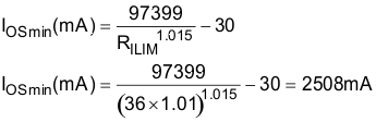
The resulting minimum current-limit threshold minimum is 2592 mA and maximum is 2894 mA with RILIM = 36 kΩ ± 1%.