SLUSCE3C October 2015 – August 2020 TPS2549-Q1
PRODUCTION DATA
- 1 Features
- 2 Applications
- 3 Description
- 4 Revision History
- 5 Pin Configuration and Functions
- 6 Specifications
- 7 Parameter Measurement Information
-
8 Detailed Description
- 8.1 Overview
- 8.2 Functional Block Diagram
- 8.3 Feature Description
- 8.4 Device Functional Modes
- 9 Application and Implementation
- 10Power Supply Recommendations
- 11Layout
- 12Device and Documentation Support
- 13Mechanical, Packaging, and Orderable Information
Package Options
Mechanical Data (Package|Pins)
- RTE|16
Thermal pad, mechanical data (Package|Pins)
- RTE|16
Orderable Information
8.3.6 CDP and SDP Auto Switch
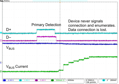
The TPS2549-Q1 device is equipped with a CDP and SDP auto-switch feature to support some popular phones in the market. These popular phones do not comply with the BC1.2 specification because they fail to establish a data connection in CDP mode. These phones use primary detection (used to distinguish between an SDP and different types of charging ports) to only identify ports as SDP (data, no charge) or DCP (no data, charge). These phones do not recognize CDP (data, charge) ports. When connected to a CDP port, these phones classify the port as a DCP and only charge the battery. Because the charging ports are configured as CDP, users do not receive the expected data connection.
 Figure 8-5 CDP and SDP Auto-Switch
To remedy this problem, the TPS2549-Q1 device employs a CDP and SDP auto-switch scheme to ensure these BC1.2 noncompliant phones establish data connection using the following steps.
- The TPS2549-Q1 device determines when a noncompliant phone has wrongly classified a CDP port as a DCP port and has not made a data connection.
- The TPS2549-Q1 device automatically completes an OUT (VBUS) discharge and reconfigures the port as an SDP.
- When reconfigured as an SDP, the phone detects a connection to an SDP and establishes a data connection.
- The TPS2549-Q1 device then switches automatically back to a CDP without doing an OUT (VBUS) discharge.
- The phone continues to operate as if connected to an SDP because OUT (VBUS) was not interrupted. The port is now ready in CDP if a new device is attached.