SLVSE57C June   2017  – April 2018 TPS2595

PRODUCTION DATA.  

  1. Features
  2. Applications
  3. Description
    1.     Device Images
      1.      Simplified Schematic
      2.      TPS25953x Overvoltage Clamp Response Time
  4. Revision History
  5. Device Comparison Table
  6. Pin Configuration and Functions
    1.     Pin Functions
  7. Specifications
    1. 7.1 Absolute Maximum Ratings
    2. 7.2 ESD Ratings
    3. 7.3 Recommended Operating Conditions
    4. 7.4 Thermal Information
    5. 7.5 Electrical Characteristics
    6. 7.6 Switching Characteristics
    7. 7.7 Typical Characteristics
  8. Detailed Description
    1. 8.1 Overview
    2. 8.2 Functional Block Diagram
    3. 8.3 Feature Description
      1. 8.3.1 Undervoltage Protection (UVP) and Undervoltage Lockout (UVLO)
      2. 8.3.2 Overvoltage Protection
        1. 8.3.2.1 Overvoltage Lockout (OVLO)
        2. 8.3.2.2 Overvoltage Clamp (OVC)
      3. 8.3.3 Inrush Current, Overcurrent and Short Circuit Protection
        1. 8.3.3.1 Slew Rate and Inrush Current Control (dVdt)
        2. 8.3.3.2 Active Current Limiting
        3. 8.3.3.3 Short Circuit Protection
      4. 8.3.4 Overtemperature Protection (OTP)
      5. 8.3.5 Fault Indication (FLT )
      6. 8.3.6 Quick Output Discharge (QOD)
    4. 8.4 Device Functional Modes
      1. 8.4.1 Enable and Fault Pin Functional Mode 1: Single Device, Self-Controlled
      2. 8.4.2 Enable and Fault Pin Functional Mode 2: Single Device, Host-Controlled
      3. 8.4.3 Enable and Fault Pin Functional Mode 2: Multiple Devices, Self-Controlled
  9. Application and Implementation
    1. 9.1 Application Information
    2. 9.2 Typical Application
      1. 9.2.1 Design Requirements
      2. 9.2.2 Detailed Design Procedure
        1. 9.2.2.1 Programming the Current-Limit Threshold: RILM Selection
        2. 9.2.2.2 Undervoltage Lockout Set Point
        3. 9.2.2.3 Setting Output Voltage Ramp Time (TdVdT)
          1. 9.2.2.3.1 Case 1: Start-Up Without Load. Only Output Capacitance COUT Draws Current
          2. 9.2.2.3.2 Case 2: Start-Up With Load. Output Capacitance COUT and Load Draw Current
      3. 9.2.3 Support Component Selection: CIN
      4. 9.2.4 Application Curves
      5. 9.2.5 Controlled Power Down (Quick Output Discharge) using TPS2595x5
      6. 9.2.6 Overvoltage Lockout using TPS259573
  10. 10Power Supply Recommendations
    1. 10.1 Transient Protection
    2. 10.2 Output Short-Circuit Measurements
  11. 11Layout
    1. 11.1 Layout Guidelines
    2. 11.2 Layout Example
  12. 12Device and Documentation Support
    1. 12.1 Documentation Support
      1. 12.1.1 Related Documentation
      2. 12.1.2 Related Links
    2. 12.2 Receiving Notification of Documentation Updates
    3. 12.3 Community Resources
    4. 12.4 Trademarks
    5. 12.5 Electrostatic Discharge Caution
    6. 12.6 Glossary
  13. 13Mechanical, Packaging, and Orderable Information

Package Options

Mechanical Data (Package|Pins)
Thermal pad, mechanical data (Package|Pins)
Orderable Information

Overvoltage Lockout using TPS259573

The TPS259573 device incorporates a circuit to protect the system during overvoltage conditions. A resistor divider connected from the supply to the EN/OVLO pin to GND (as shown in Figure 65) programs the overvoltage threshold. A voltage more than VOVLO on the EN/OVLO pin turns off the internal FET and protects the downstream load. Figure 66 shows overvoltage cut-off at the input voltage of 15 V.
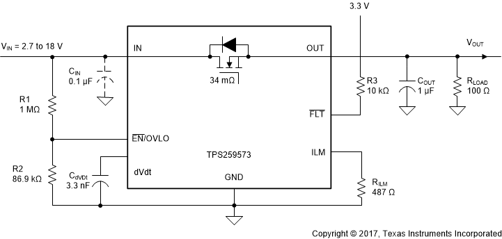
TPS2595 tps2595x-circuit-implementation-for-overvoltage-lockout-block-diagram.gifFigure 65. Circuit Implementation for Overvoltage Lockout using TPS259573
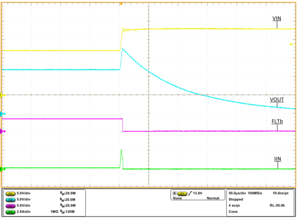
TPS2595 tps2595x-overvoltage-lockout-response-using-tps2595x3-efuse-scope-shot.gifFigure 66. Overvoltage Lockout Response using TPS259573