SLVSE94F September 2018 – June 2021 TPS2663
PRODUCTION DATA
- 1 Features
- 2 Applications
- 3 Description
- 4 Revision History
- 5 Device Comparison Table
- 6 Pin Configuration and Functions
- 7 Specifications
- 8 Parameter Measurement Information
-
9 Detailed Description
- 9.1 Overview
- 9.2 Functional Block Diagram
- 9.3
Feature Description
- 9.3.1 Hot Plug-In and In-Rush Current Control
- 9.3.2 PGOOD and PGTH
- 9.3.3 Undervoltage Lockout (UVLO)
- 9.3.4 Overvoltage Protection (OVP)
- 9.3.5 Input Reverse Polarity Protection (B_GATE, DRV)
- 9.3.6 Reverse Current Protection
- 9.3.7 Overload and Short Circuit Protection
- 9.3.8 Output Power Limiting, PLIM (TPS26632, TPS26633, TPS26635 and TPS26636 Only)
- 9.3.9 Current Monitoring Output (IMON)
- 9.3.10 FAULT Response ( FLT)
- 9.3.11 IN_SYS, IN, OUT and GND Pins
- 9.3.12 Thermal Shutdown
- 9.3.13 Low Current Shutdown Control (SHDN)
- 9.4 Device Functional Modes
-
10Application and Implementation
- 10.1 Application Information
- 10.2
Typical Application: Power Path Protection in a PLC System
- 10.2.1 Design Requirements
- 10.2.2 Detailed Design Procedure
- 10.2.3 Application Curves
- 10.3 System Examples
- 10.4 Do's and Don'ts
- 11Power Supply Recommendations
- 12Layout
- 13Device and Documentation Support
- 14Mechanical, Packaging, and Orderable Information
Package Options
Refer to the PDF data sheet for device specific package drawings
Mechanical Data (Package|Pins)
- RGE|24
- PWP|20
Thermal pad, mechanical data (Package|Pins)
Orderable Information
3 Description
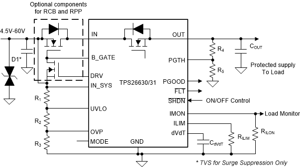
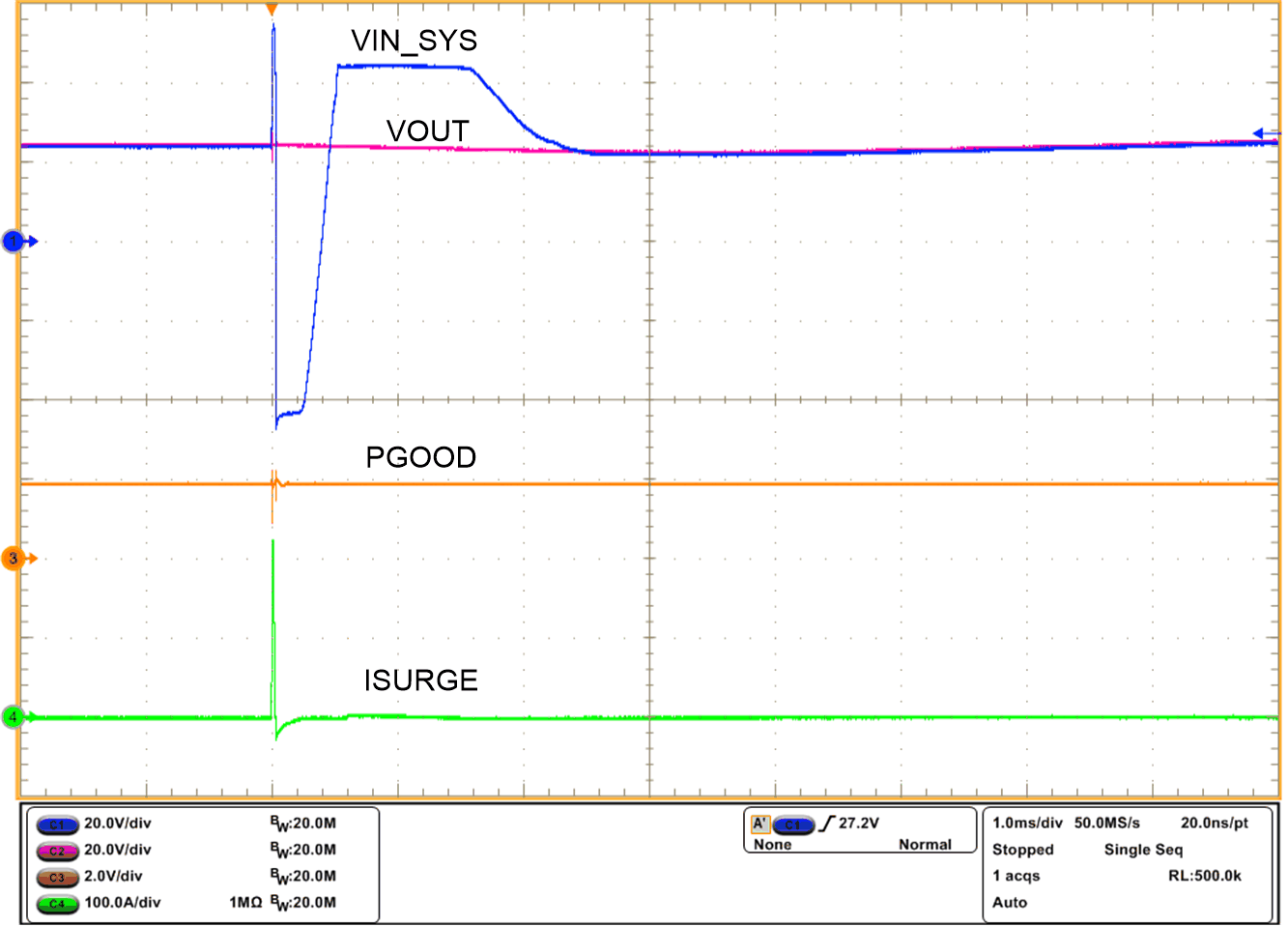
The TPS2663x devices are easy to use, positive 60 V and 6-A eFuse with a 31-mΩ integrated FET. It features a B-FET driver to control an external N-channel FET in the system designs that require protection from input reverse polarity faults and reverse current blocking. The device incorporates robust protection features that simplify system designs requiring protection during system tests like IEC61000-4-5 industrial surge tests. The device features an adjustable output power limiting (PLIM) functionality that simplifies the system design requiring compliance in accordance to the standards like IEC61010-1 and UL1310. Additional protection features include adjustable overcurrent protection, fast short circuit protection, output slew rate control, overvoltage protection and undervoltage lockout.
For system status monitoring and downstream load control, the device provides fault and a precise current monitor output. PGOOD can be used for enable and disable control of the downstream DC-DC converters. The MODE pin allows flexibility to configure the device between the two current-limiting fault responses (latch off and auto-retry).
| PART NUMBER | PACKAGE | BODY SIZE (NOM) |
|---|---|---|
| TPS26630 TPS26631 TPS26632 TPS26633 TPS26635 |
VQFN (24) | 4.00 mm × 4.00 mm |
| TPS26631 TPS26633 TPS26636 |
HTSSOP (20) | 6.50 mm × 4.40 mm |
 Simplified Schematic
 IEC61000-4-5 Surge
Performance at 24-V Supply