SLVS363G August 2001 – September 2016 TPS3103 , TPS3106 , TPS3110
PRODUCTION DATA.
- 1 Features
- 2 Applications
- 3 Description
- 4 Revision History
- 5 Available Options
- 6 Pin Configuration and Functions
- 7 Specifications
- 8 Detailed Description
- 9 Application and Implementation
- 10Power Supply Recommendations
- 11Layout
- 12Device and Documentation Support
- 13Mechanical, Packaging, and Orderable Information
Package Options
Refer to the PDF data sheet for device specific package drawings
Mechanical Data (Package|Pins)
- DBV|6
Thermal pad, mechanical data (Package|Pins)
Orderable Information
7 Specifications
7.1 Absolute Maximum Ratings
over operating junction temperature range (unless otherwise noted)(1)| MIN | MAX | UNIT | ||
|---|---|---|---|---|
| Supply voltage(2) | VDD | –0.3 | 4 | V |
| MR Pin, RESET (push-pull) | VMR, VRESET (push-pull) | –0.3 | VDD + 0.3 | V |
| All other pins(2) | –0.3 | 4 | V | |
| Maximum low output current | IOL | –5 | 5 | mA |
| Maximum high output current | IOH | –5 | 5 | mA |
| Input current | IIK (VSENSE < 0 V or VSENSE > VDD) | –10 | 10 | mA |
| Output current | IOK (VO < 0 V or VO > VDD)(3) | –10 | 10 | mA |
| Continuous total power dissipation | See Thermal Information | |||
| Temperature | Operating, TJ | –40 | 125 | °C |
| Storage, Tstg | –65 | 150 | °C | |
(1) Stresses beyond those listed under Absolute Maximum Ratings may cause permanent damage to the device. These are stress ratings only, which do not imply functional operation of the device at these or any other conditions beyond those indicated under Recommended Operating Conditions. Exposure to absolute-maximum-rated conditions for extended periods may affect device reliability.
(2) All voltage values are with respect to GND. For reliable operation, the device must not be operated at 3.6 V for more than t = 1000h continuously.
(3) Output is clamped for push-pull outputs by the back gate diodes internal to the IC. No clamp exists for the open-drain outputs.
7.2 ESD Ratings
| VALUE | UNIT | |||
|---|---|---|---|---|
| V(ESD) | Electrostatic discharge | Human body model (HBM), per ANSI/ESDA/JEDEC JS-001, all pins(1) | ±2000 | V |
| Charged device model (CDM), per JEDEC specification JESD22-C101, all pins(2) | ±500 | |||
(1) JEDEC document JEP155 states that 500-V HBM allows safe manufacturing with a standard ESD control process.
(2) JEDEC document JEP157 states that 250-V CDM allows safe manufacturing with a standard ESD control process.
7.3 Recommended Operating Conditions
over operating junction temperature range, unless otherwise noted.| MIN | NOM | MAX | UNIT | ||
|---|---|---|---|---|---|
| VDD(1) | Supply voltage | 0.9 | 3.6 | V | |
| VSENSE | SENSE voltage | 0 | VDD | V | |
| WDI | High-level input voltage VIH at MR | 0.7 × VDD | V | ||
| WDI | Low-level input voltage VIL at MR | 0.3 × VDD | V | ||
| WDI | Input transition rise and fall rate at Δt/ΔV at MR | 100 | ns/V | ||
| MR | MR voltage | 0 | VDD | V | |
| PFI | PFI voltage | 0 | 3.6 | V | |
| TJ | Operating temperature | –40 | 125 | °C | |
(1) For proper operation of SENSE, PFI, and WDI functions: VDD ≥ 0.8 V.
7.4 Thermal Information
| THERMAL METRIC(1) | TPS31xx | UNIT | |
|---|---|---|---|
| DBV (SOT-23) | |||
| 6 PINS | |||
| RθJA | Junction-to-ambient thermal resistance | 183.2 | °C/W |
| RθJC(top) | Junction-to-case (top) thermal resistance | 123.3 | °C/W |
| RθJB | Junction-to-board thermal resistance | 29.4 | °C/W |
| ψJT | Junction-to-top characterization parameter | 20.5 | °C/W |
| ψJB | Junction-to-board characterization parameter | 29 | °C/W |
(1) For more information about traditional and new thermal metrics, see the Semiconductor and IC Package Thermal Metrics application report, SPRA953.
7.5 Electrical Characteristics
over operating junction temperature range (unless otherwise noted).| PARAMETER | TEST CONDITIONS | MIN | TYP | MAX | UNIT | ||
|---|---|---|---|---|---|---|---|
| VOH | High-level output voltage | VDD = 3.3 V, IOH = –3 mA | 0.8 × VDD | V | |||
| VDD = 1.8 V, IOH = –2 mA | |||||||
| VDD = 1.5 V, IOH = –1 mA | |||||||
| VDD = 0.9 V, IOH = –0.4 mA | |||||||
| VDD = 0.5 V, IOH = –5 μA | 0.7 × VDD | ||||||
| VOL | Low-level output voltage | VDD = 3.3 V, IOL = 3 mA | 0.3 | V | |||
| VDD = 1.5 V, IOL = 2 mA | |||||||
| VDD = 1.2 V, IOL = 1 mA | |||||||
| VDD = 0.9 V, IOL = 500 μA | |||||||
| VOL | Low-level output voltage | RESET only | VDD = 0.4 V, IOL = 5 μA | 0.1 | V | ||
| VIT– | Negative-going input threshold voltage(1) | TPS31xxE09 | TA = 25°C | 0.854 | 0.86 | 0.866 | V |
| TPS31xxE12 | 1.133 | 1.142 | 1.151 | ||||
| TPS31xxE15 | 1.423 | 1.434 | 1.445 | ||||
| TPS31xxE16 | 1.512 | 1.523 | 1.534 | ||||
| TPS31xxH20 | 1.829 | 1.843 | 1.857 | ||||
| TPS31xxK33 | 2.919 | 2.941 | 2.963 | ||||
| TPS31xxE09 | TA = –40°C to 125°C | 0.817 | 0.903 | ||||
| TPS31xxE12 | 1.084 | 1.199 | |||||
| TPS31xxE15 | 1.362 | 1.505 | |||||
| TPS31xxK33 | 2.823 | 3.058 | |||||
| VIT–(S) | Negative-going input threshold voltage(1) | SENSE, PFI | VDD ≥ 0.8 V, TA = 25°C | 0.542 | 0.551 | 0.559 | V |
| VDD ≥ 0.8 V, TA = –40°C to 125°C | 0.5 | 0.58 | |||||
| VHYS | Hysteresis at VDD input | 0.8 V ≤ VIT– < 1.5 V | 20 | mV | |||
| 1.6 V ≤ VIT– < 2.4 V | 30 | ||||||
| 2.5 V ≤ VIT– < 3.3 V | 50 | ||||||
| T(K) | Temperature coefficient of VIT−, PFI, SENSE | TA = –40°C to 85°C | –0.012 | –0.019 | %/K | ||
| VHYS(S) | Hysteresis at SENSE, PFI input | VDD ≥ 0.8 V | 15 | mV | |||
| IIH | High-level input current | MR | MR = VDD, VDD = 3.3 V | –25 | 25 | nA | |
| SENSE, PFI, WDI | SENSE, PFI, WDI = VDD, VDD = 3.3 V |
–25 | 25 | ||||
| IIL | Low-level input current | MR | MR = 0 V, VDD = 3.3 V | –47 | –33 | –25 | μA |
| SENSE, PFI, WDI | SENSE, PFI, WDI = 0 V, VDD = 3.3 V |
–25 | 25 | nA | |||
| IOH | High-level output current at RESET(2) | Open-drain | VDD = VIT– + 0.2 V, VOH = 3.3 V | 200 | nA | ||
| IDD | Supply current | TA = –40°C to 85°C, VDD > VIT– (average current), VDD < 1.8 V | 1.2 | 3 | μA | ||
| TA = –40°C to 125°C, VDD > VIT– (average current), VDD < 1.8 V | 3 | ||||||
| TA = –40°C to 85°C, VDD > VIT– (average current), VDD > 1.8 V | 2 | 4.5 | |||||
| TA = –40°C to 125°C, VDD > VIT– (average current), VDD > 1.8 V | 5.5 | ||||||
| TA = –40°C to 85°C, VDD < VIT–, VDD < 1.8 V | 22 | ||||||
| TA = –40°C to 125°C, VDD < VIT–, VDD < 1.8 V | 27 | ||||||
| TA = –40°C to 85°C, VDD < VIT–, VDD > 1.8 V | 27 | ||||||
| TA = –40°C to 125°C, VDD < VIT–, VDD > 1.8 V | 32 | ||||||
| Internal pullup resistor at MR | 70 | 100 | 130 | kΩ | |||
| CIN | Input capacitance at MR, SENSE, PFI, WDI | VIN = 0 V to VDD | 1 | pF | |||
(1) To ensure the best stability of the threshold voltage, a bypass capacitor (ceramic, 0.1 μF) should be placed close to the supply terminals.
(2) Also refers to RSTVDD and RSTSENSE.
7.6 Timing Requirements
At RL = 1 MΩ, CL = 50 pF, and TA = –40°C to 85°C, unless otherwise noted.| MIN | TYP | MAX | UNIT | ||||
|---|---|---|---|---|---|---|---|
| tT(OUT) | Time-out period | at WDI | VDD ≥ 0.85 V | 0.55 | 1.1 | 1.65 | s |
| tW | Pulse duration | at VDD | VIH = 1.1 × VIT–, VIL = 0.9 × VIT–, VIT– = 0.86 V | 20 | μs | ||
| at MR | VDD ≥ VIT– + 0.2 V, VIL = 0.3 × VDD, VIH = 0.7 × VDD | 0.1 | |||||
| at SENSE | VDD ≥ VIT–, VIH = 1.1 × VIT − (S), VIL = 0.9 × VIT − (S) | 20 | |||||
| at PFI | VDD ≥ 0.85 V, VIH = 1.1 × VIT − (S),VIL = 0.9 × VIT − (S) | 20 | |||||
| at WDI | VDD ≥ VIT–, VIL = 0.3 × VDD, VIH = 0.7 × VDD | 0.3 | |||||
7.7 Switching Characteristics
At RL = 1 MΩ, CL = 50 pF, and TA = –40°C to 85°C, unless otherwise noted.| PARAMETER | TEST CONDITIONS | MIN | TYP | MAX | UNIT | ||
|---|---|---|---|---|---|---|---|
| tD | Delay time | VDD ≥ 1.1 × VIT–, MR = 0.7 × VDD. See Timing Requirements. |
65 | 130 | 195 | ms | |
| tPHL(VDD) | Propagation delay time, high-to-low level output |
VDD to RESET or RSTVDD delay | VIH = 1.1 × VIT–, VIL = 0.9 × VIT– | 40 | μs | ||
| tPHL(SENSE) | Propagation delay time, high-to-low level output |
SENSE to RESET or RSTSENSE delay | VDD ≥ 0.8 V, VIH = 1.1 × VIT–, VIL = 0.9 × VIT– | 40 | μs | ||
| tPHL(PFO) | Propagation delay time, high-to-low level output |
PFI to PFO delay | VDD ≥ 0.8 V, VIH = 1.1 × VIT–, VIL = 0.9 × VIT– | 40 | μs | ||
| tPLH(PFO) | Propagation delay time, low-to-high level output |
PFI to PFO delay | VDD ≥ 0.8 V, VIH = 1.1 × VIT–, VIL = 0.9 × VIT– | 300 | μs | ||
| tPHL(MR) | Propagation delay time, high-to-low level output |
MR to RESET. RSTVDD, RSTSENSE delay | VDD ≥ 1.1 × VIT–, VIL = 0.3 × VDD, VIH = 0.7 × VDD | 1 | 5 | μs | |
7.8 Typical Characteristics
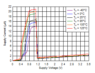 Figure 5. TPS3110E09 Supply Current vs Supply Voltage
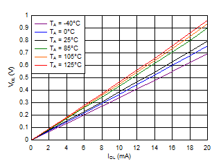
| VDD = 3.3 V, SENSE = GND, MR = GND, WDI: GND |
Low-Level Output Current
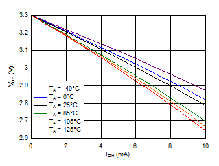
| VDD = 3.3 V, SENSE = VDD, MR = VDD, WDI: triggered |
High-Level Output Current
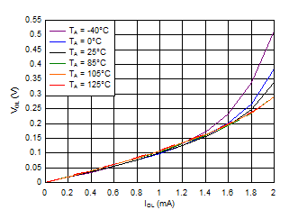
| VDD = 0.9 V, SENSE = GND, MR = GND, WDI: GND |
Low-Level Output Current
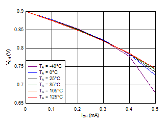
| VDD = 0.9 V, SENSE = VDD, MR = VDD, WDI: triggered |
High-Level Output Current
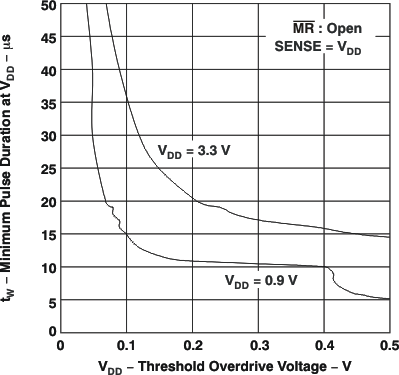
Threshold Overdrive Voltage
